Issued Date:2026/01/20 High Speed Ethernet
Issued By:iST
As 400G/800G Ethernet transitions from the datasheet to mass production, many R&D teams are facing a frustrating paradox: simulations look perfect, and IC specifications meet the standard, but the final product fails to reach maximum throughput. Is the root cause in the design itself, the physical channel characteristics, or the test condition settings? Why is High-Speed Ethernet so difficult to verify?
High Speed Ethernet
High Speed Ethernet
At CES 2026, NVIDIA CEO Jensen Huang officially unveiled the new Vera Rubin architecture. Its computational performance has surged fivefold compared to the previous Blackwell generation, pushing data center networks toward the extreme bandwidth limit of 1.6T (Terabit Ethernet).
With the industry leader defining the next era of transmission, the focus shifts back to the current peak of mass production: 400G/800G Ethernet. The Signal Integrity (SI) challenge has evolved beyond mere “compliance.” The real key now lies in ensuring sufficient Signal Margin under high-bandwidth conditions.
In this evolution, high-speed Ethernet is no longer just about doubling bandwidth; the difficulty of SI verification has grown exponentially.
In the early stages of high-speed product design, Signal Integrity (SI) simulation is an indispensable first step. (Read more: Why SIPI Simulation Is Becoming Essential in High-Speed Product Design ) It assists R&D teams in architecture optimization and risk assessment. However, under the 100G/lane PAM4 architecture, the tolerance for physical channels, connectors, and test conditions has been compressed to the absolute limit. Any minor impedance discontinuity, material variation, equalizer setting offset, or test calibration error can be amplified into a systemic risk during the physical testing phase.
Driven by the deployment of NVIDIA H100/H200, Blackwell, and now Vera Rubin—alongside expanding AI infrastructure from AMD and cloud giants like Google—maintaining high-speed, stable bandwidth has become a standard for hardware survival. This makes 400G/800G Ethernet signal verification the critical gateway for AI systems to successfully enter mass production and bridge the gap to future 1.6T standards.
This edition of “iST Tech Classroom” focuses on the empirical verification of 400G/800G Ethernet. We will explore TX (Transmitter), RX (Receiver), and S-Parameter testing to share common critical challenges and help you break through the final line of defense before mass production.
In the 400G/800G era, the single-lane data rate has climbed to a staggering 112G PAM4. At such high frequencies, signals are hyper-sensitive to Insertion Loss (IL), Reflection, and Crosstalk. Any minor impedance discontinuity is infinitely magnified in Eye Diagram or Bit Error Rate (BER) performance. From connectors and PCB trace layouts to material properties, every detail directly impacts signal integrity.
To survive these harsh conditions, R&D must supplement software simulation with physical testing, strictly following IEEE 802.3 standards across TX and RX domains to ensure adequate design margin. Below, we break down how iST Laboratory helps clients conquer these hurdles through three representative testing scenarios.
I. TX (Transmitter) Validation: Equalization Optimization
At 100Gbps per lane, signal attenuation is severe. To compensate, IEEE 802.3 established a more complex Transmitter Equalizer (TXEQ) to meet these high-speed standards.
1. The “Parameter Maze” of 5-tap EQ
Under 112G PAM4, signal decay is violent. IEEE 802.3ck upgraded the TXEQ from a traditional 3-tap to a 5-tap FIR filter. Simultaneously, the Receiver (RXEQ) CTLE (Continuous Time Linear Equalizer) was enhanced to a second-order design (gdc + gdc2). While this significantly boosts compensation, it introduces a massive combination of parameters. Manually attempting to find the optimal tap values and coefficients is nearly impossible.
2. Beyond “Pass”: Insights into Design Resilience
In 800G TX validation, a ‘Pass’ is merely the baseline—like scoring a 70% on an exam. It meets the requirement, but leaves little room for error if the environment fluctuates. By analyzing precise waveforms, engineers can determine if a ‘Pass’ has a healthy margin (e.g., a ’90-point’ score) or is barely scraping by with a ’71’. This precision is vital for ensuring cross-device compatibility in complex systems.
3. The iST Solution: Automated Precision Locking
To shorten testing cycles, iST Signal Integrity Lab utilizes a high bandwidth oscilloscope platform combined with automated testing workflows. This allows for the rapid identification of the optimal EQ parameter combination, providing stable, reproducible results that help engineers confirm design quality on schedule.
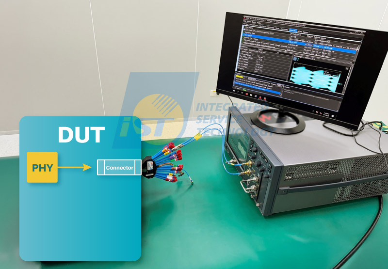
Figure 1: 100GAUI C2M Host TX Test Setup.
(Source:iST)II. RX (Receiver) Validation: Calibration as the Lifeline
While TX validation evaluates output quality, RX validation asks: When a signal is severely degraded after traveling through a long channel, can the product still interpret the data correctly?
1. The Standard: Crafting a Precise “Stressed Signal Source”
The hardest part of RX testing is Stressed Signal Calibration. To test a receiver’s tolerance limits, we cannot provide a clean signal. We must intentionally introduce specific amounts of Jitter, Interference, and Noise. If the signal is too clean, everyone passes; if it’s too noisy, everyone fails. To ensure discriminative results, iST Signal Integrity Lab locks the signal precisely at the regulatory boundary—such as an Eye Height (EH) of 15mV and a Vertical Eye Closure (VEC) of 12dB.
2. The Hidden Challenge: Eliminating Environment Bias
If calibration is imprecise, an abnormal BER leaves R&D in a stalemate: Is the chip design flawed, or is the test equipment providing a non-compliant signal? This uncertainty often halts R&D progress.
3. The iST Solution: High-Precision Automated Calibration
iST Signal Integrity Lab employs a high-precision receiver test platform with automated software to perform RX signal calibration, ensuring absolute accuracy and consistency while eliminating human error.
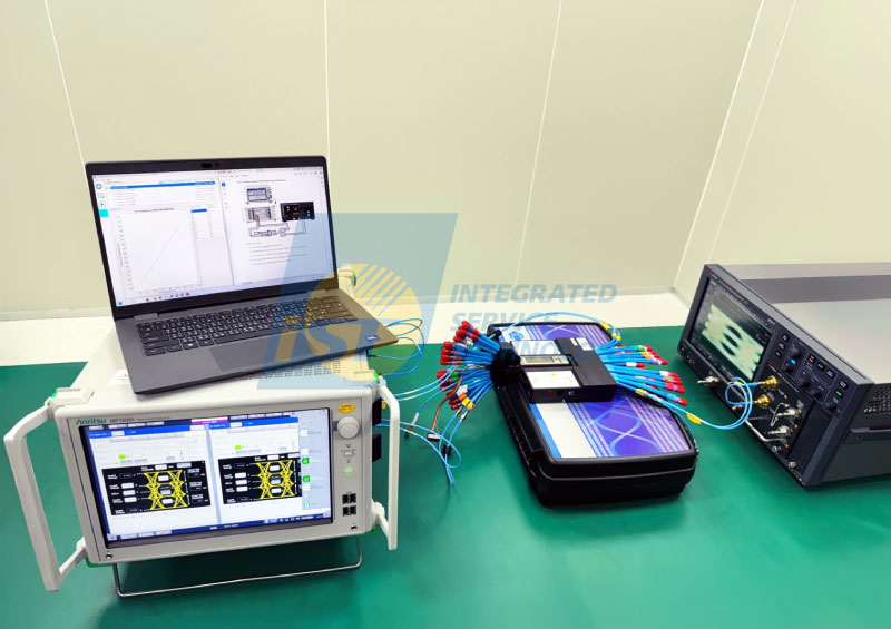
Figure 2: 100GAUI C2M Host RX Signal Calibration Setup.
(Source: iST)III. Specialized RX Validation: ISI Board Stress Testing
In C2C (Chip-to-Chip), CR (Copper Cable), or KR (Backplane) architectures, signals must traverse complex PCB traces, backplanes or long cables. This requires a different validation flow.
1. ISI Board: Restoring Realistic Link Loss
IEEE 802.3ck specifies the use of an ISI Board (Inter-Symbol Interference Board) to simulate signal attenuation over long distances. This board must provide precise, controlled Insertion Loss. If the ISI board design or material is substandard, the RX test is like racing on the wrong track—the data becomes meaningless.
2. COM Analysis: The Ticket to Stress Testing
Before RX validation, engineers must extract S-Parameters (Scattering Parameters) from the ISI board and link, then calculate the COM (Channel Operating Margin) value. According to the specification, COM must be > 3dB. Only then is the ISI board considered compliant for further testing. This ensures that the RX validation happens under “reasonable” channel conditions rather than idealized ones.
3. The iST Solution: High Bandwidth VNA and Standardized ISI Channels
iST Signal Integrity Lab utilizes a 67GHz Vector Network Analyzer (VNA) to capture the intricate S-parameter details required for 800G specifications. Combined with compliant ISI simulation boards, this setup guarantees the accuracy of the S-parameter data and the overall RX test result.
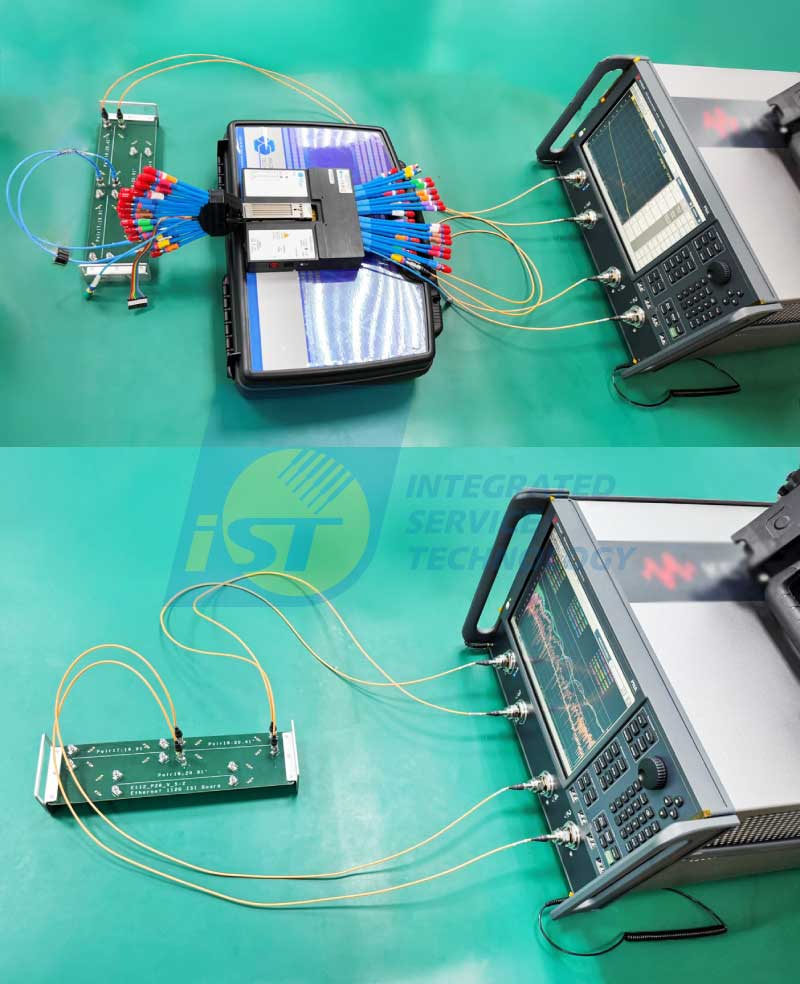
Figure 3: 800G Ethernet RX Validation S-Parameter Measurement Setup.
(Source: iST)
With the arrival of NVIDIA’s Vera Rubin and the Spectrum-6 1.6T switch, AI interconnect bandwidth has entered “deep water” territory. While Blackwell set a high bar, the signal margins for 800G are becoming increasingly marginal. However, stable 800G testing is the mandatory path to the 1.6T challenge.
From 400G to 800G and the looming 1.6T era, validation is no longer just about “checking a box”—it is critical risk management. Even microscopic signal distortion can lead to massive system-wide efficiency drops.
Precise empirical data, rigorous stress calibration, and COM analysis are the keys to keeping your products stable amidst the AI wave.
iST Signal Integrity Lab continues to share first-hand observations and case studies to help R&D teams eliminate signal hazards and lead the way in mass production.
For further consultation or technical details, please contact us:
+886-2-2792-2890 ext. 2715 Mr. David Chen Email: web_si@istgroup.com;marketing_tw@istgroup.com