Issued Date:2023/9/12 FFT
Issued By:iST

High-end TEM sample costs can be steep, yet analyzing the atomic-level details of heterogeneous material interfaces is crucial. Is there a way to balance cost and need?
This article presents two cases demonstrating the use of Fourier filtering techniques to enhance HRTEM image quality in TEM samples at a relatively lower cost, while delving into atomic-scale analysis of diverse crystal interfaces.
FFT
In our previous “Uncle Bow’s Corner” (read more: Five Case Studies Unveil What You Don’t Know About TEM Material Analysis), the Fourier image filtering technique was briefly introduced. This technique enhances the clarity of High-Resolution TEM (HRTEM) images. Here, we will delve further into this image processing technique and share two case studies that demonstrate how it is utilized for analyzing heterogeneous crystal interfaces. This will help you strike a balance between cost and demand.
FFT
FFT
1. Real Space and Reciprocal Space in TEM
There are two basic analytical functions for TEM instruments: electron diffraction and imaging. Structures of materials shown in TEM images are real structures and are almost identical in images obtained by other microscopes. The space where objects exist is called real space in electron microscopy. Real space is a 3D space which we are familiar with. TEM electron diffraction patterns are products of interaction of waves of incident high energy electrons and specimens. We call the space where electron diffraction spots exist the reciprocal space[1 ~ 3].
After passing through the thin foil specimen, high energy electrons form a set of diffraction pattern at the back focal plane of the objective lenses, the morphology and intensity variation of diffraction spots have specified relationships with the structure of atoms and crystal of specimens. The process of transferring electrons leaving the specimen to a set of electron diffraction pattern can be described by the Fourier function. Thus, the transfer is called Fourier transfer. In TEM, the transfer is a three-dimensional transformation and very complicated.
Only two-dimensional Fourier transfer of HRTEM images, is discussed in this article. The function used to Fourier transform HRTEM images in the TEM image process software package is called fast Fourier transformation and is abbreviated as FFT in general.
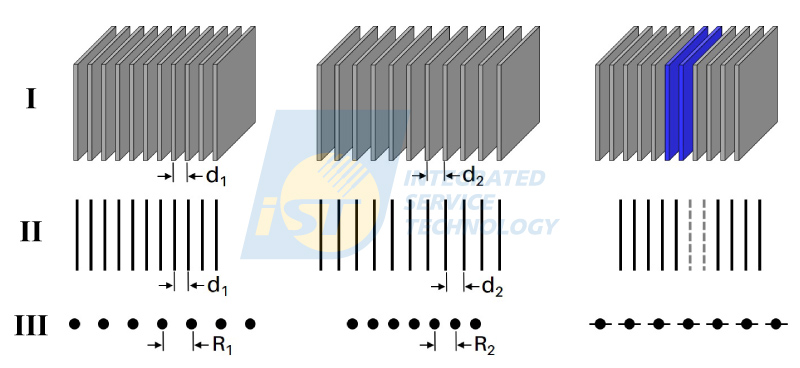
Figure 1: Schematical diagram of the basic FFT of HRTEM images. There are three sets of crystal planes in (a)(b)(c) respectively. Row I: crystal planes, row II: lattice fringes of crystal planes in HRTEM images, row III: FFT patterns of lattice fringes.
The basic concept of Fourier transformation is illustrated in Figure 1. Once a set of crystal planes (Figure 1, row I) are parallel to the incident beam, a set of parallel lattice fringes will be formed at the TEM image plane and become visible in acquired TEM images when the magnification is large enough (usually > 100 KX), and the spacing of these fringes is equal to the d-spacing of this set of crystal planes, d (the spacing of crystal planes in TEM image). The FFT pattern of this set of fringes is a set of spots in a line. The spacing of these spots, R (the distance between the transmitted beam and diffraction beams in TEM electron diffraction patterns), is inversely proportional to d, as shown in Figure 1(a) and (b). If a few of crystal planes are different from others in composition and/or crystal structure and form an ultra-thin structure, there will be a set of corresponding streaks in the FFT pattern, as shown in Figure 1(c).
2. Real Space and Reciprocal Space, Large is Small and Vice Versa
Figure 2 shows two sets of Si [110] HRTEM images and corresponding diffractograms (FFT patterns) of different magnification. Due to images exist in the real space and diffractograms exist in the reciprocal space, distances of lattice fringes increase with the magnification of HRTEM images, while distances of spots in diffractograms decrease with it.
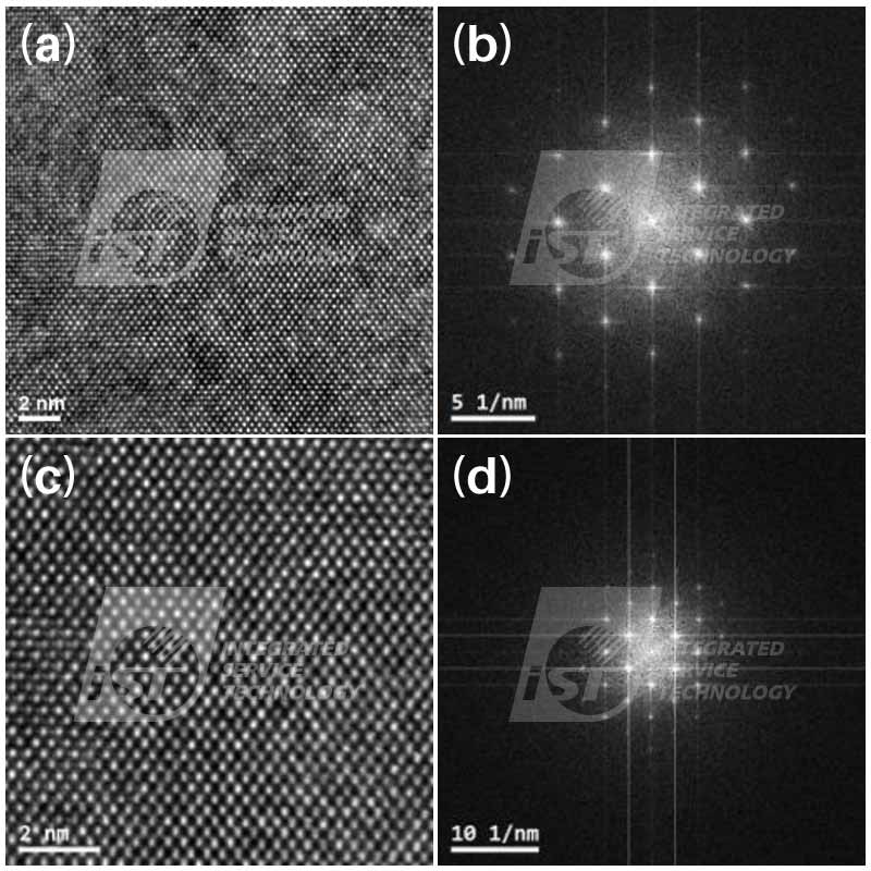
Figure 2: HRTEM images and corresponding diffractograms. (a) & (b) 250 KX, (c) & (d) 500 KX.
We find that the background intensity around spots in diffractograms is grey rather than dark when we check FFT patterns carefully. It means that some noise signals among atoms in HRTEM images. Those noise signals locate at central region of the FFT pattern are called low frequency noise because the “wave lengths” of these signals are longer than d-spacings. All signals locate outside diffraction spots of the first level are called high frequency noises because the “wave lengths” of these signals are shorter than d-spacings. Parts of sources of noises result from the quality of TEM specimens, including specimen thickness, roughness of the specimen surfaces, thickness of surface damage layers, etc. The cost is very high to prepare a TEM specimen of ultra-high quality (the specimen thickness is thinner than 60 nm, flat and no bending at all, the thickness of surface damage layers less than 1 nm), since advanced operating technology and expensive instruments are both required, especially for semiconductor specimens of specified site types. Roughly, the cost is two to three times of present ones.
On the other hand, the cost of using the Fourier filtering technique to enhance the clarity of HRTEM images is much lower. Requirements for analyzers who perform the filtering job are to have knowledge of HRTEM and material crystallography and know how to operate DigitalMicroph[4]well. As shown in Figure 3, the HRTEM image is Fourier transformed to get a set of FFT pattern firstly, then a group of proper masks are set to filter off noises of low and high frequency, finally a filtered HRTEM image (Figure 3(d)) is obtained by inverse FFT. No visible noise among atoms is observed in the filtered HRTEM image, and the brightness of all atoms are almost same. The vague atomic structure of interface of two heterogeneous crystals, caused by strain, can be made clear again by this filtering technique. Distinct HRTEM images of crystal interfaces will reveal more material information to atomic scale.
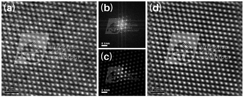
Figure 3: Basic procedure of Fourier filtering. (a)HRTEM image, (b)FFT pattern, (c)mask applied FFT pattern, (d)Fourier filtered HRTEM image.
3. Border of Heterogeneous Crystals I: Ti/6H-SiC
Both titanium (Ti) metal and 6H-SiC are hexagonal crystals. An epitaxial Ti thin film can be obtained by depositing Ti on a (0001) 6H-SiC substrate using molecular beam epitaxy (MBE). The crystallographic relationship between them are (0001)Ti // (0001)6H-SiC,and (1 -100)Ti // (1 -100)6H-SiC[5]. Because the d-spacing of (1 -100) Ti (0.2557 nm) is a little smaller than that of (1 -100)6H-SiC (0.2660 nm), a stress, resulting from this lattice mismatch, exist at the interface and makes those atoms around the interface vague in HRTEM images. This is a common phenomenon in HRTEM images of interfaces of heterogenous crystals.
Quality of this kind of HRTEM images can be much improved by applying Fourier filtering to filter out noises. In Figure 4(b), a yellow dash line draws the position of the interface of Ti/6H-SiC, the region below this yellow dash line is the 6H-SiC substrate. This dash line is not a straight line along a same (0006)6H-SiC plane. There is a step, a layer of (0006)6H-SiC plane high, close to the right side. This kind of steps supply low energy nucleation sites for epitaxial thin films growth during early stage of epitaxial thin film growth. Strains resulted from lattice mismatches of (1 -100) Ti and (1 -100)6H-SiC as well as Ti (0002) Ti and (0006)6H-SiC are relaxed by Ti atoms at the corner of the step. That is why Ti atoms (marked by a white arrow) at this place are so fuzzy in the original HRTEM image. Ti atoms in the filtered HRTEM image are much clear, and an extra (0002) Ti crystal plane at the left side of the step is observed.
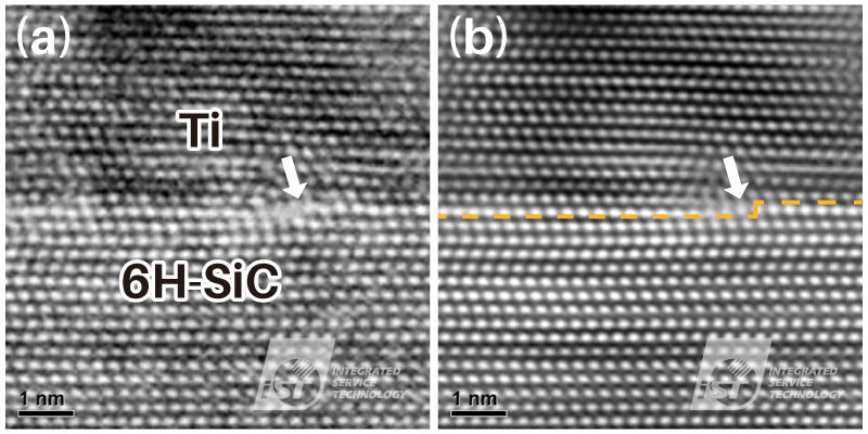
Figure 4: HRTEM images of Ti/6H-SiC. (a) raw HRTEM image, (b) Fourier filtered HRTEM image.
Although the d-spacing of (1 -100) Ti is a little smaller than that of (1 -100)6H-SiC, the first layer of Ti atoms locate upon those Si-C atoms site on the 6H-SiC substrate one by one. This result indicates that the ductility of titanium can relax the strain. This strain energy increases the energy of the interface, on the other hand, the surface energy of a heterointerface reduces with a flat interface replacing a rough interface. It is deduced that reduce in surface energy is larger than increase in strain energy for this material system from this HRTEM image. There are still some fuzzy Ti atoms observed somewhere in the first four Ti (0002) layers in the filtered HRTEM image. This indicates that strains of certain levels exist in these four Ti (0002) layers. The distortion of Ti atoms in the fifth (0002) layer and layers behind are negligible in this HRTEM image. It is deduced that the strain, caused by 3.87% lattice mismatch between Ti {1 -100} and 6H-SiC {1 -100}, in the Ti thin film is gradually relaxed by four Ti (0002) layers.
4. Border of heterogeneous crystals II: ZnSi/Si (111)
Quantum dots (QD) of Zinc (Zn) was deposited on a (111) Si substrate by using Radio-Frequency Sputtering [6]. Zn quantum dots formed on the Si surface during deposition. The original HRTEM image of Zn QD/Si is not clear enough to analyze the crystal structure of this Zn QD and the interface structure of Zn QD/Si. They can be made much clear after applying the Fourier filtering to the HRTEM image to filter noise among atoms, as shown in Figure 5.
![Quantum dots (QD) of Zinc (Zn) was deposited on a (111) Si substrate by using Radio-Frequency Sputtering [6]. Zn quantum dots formed on the Si surface during deposition. The original HRTEM image of Zn QD/Si is not clear enough to analyze the crystal structure of this Zn QD and the interface structure of Zn QD/Si. They can be made much clear after applying the Fourier filtering to the HRTEM image to filter noise among atoms, as shown in Figure](https://www.istgroup.com/en/wp-content/uploads/2023/09/tech_20230921-05-TEMFFT-1.jpg)
Figure 5: HRTEM image of Zn silicide/Si. (a) original HRTEM image, (b)Fourier filtered HRTEM image, (c) magnified HRTEM image of the yellow rectangle in (b). (Source: HRTEM Image of Zn Silicide/Si provided by Professor Kuang-Yao Lo, Department of Physics, National Cheng Kung University.)
More and more dissimilar materials are being joined in the semiconductor industry to fulfill functional requirements. Following, more and more engineering problems are being encountered in heterogeneous material joining. It is a trend to analyze these interfaces to atomic scale to fully understand what happened in materials join. At present, it is not a problem to analyze these interfaces to atomic scale for the resolution power of current TEMs. But there are still some barriers in preparing ultra-high quality TEM specimens to make atoms around the interfaces very clear in all HRTEM images. The price is still very high to build up those precision instruments and to train skilled engineers for this kind of work currently. The cost of obtaining high quality of HRTEM images to analyze heterointerfaces to the atomic scale can be much reduced by using the off-line TEM Fourier filtering technique.
References:
[1] J. W. Edington, in Practical Electron Microscopy in Materials Science, published by Van Nostrand Reinhold Company, New York (1976).
[2] G. Thomas and M. J. Goringe, Transmission Electron Microscopy of Materials, John Wiley & Sons, Inc., New York (1979).
[3] David B. Williams and C. Barry Carter, in Transmission Electron Microscopy, Microscopy, part 2, Plenum Press, New York (2007).
[4] B. Schaffer, in Transmission Electron Microscopy, Microscopy, chapter 6, Springer International Publishing, Switzerland (2016).
[5] L.M. Porter, et.al., “Chemistry, microstructure, and electrical properties at interfaces between thin films of titanium and alpha (6H) silicon carbide (0001),” J. Mater. Res., Vol.10, No. 3 (1995).
[6] B. J. Huang et.al., “Epitaxial Zn quantum dots coherently grown on Si(1 1 1): growth mechanism, nonlinear optical and chemical states analyses,” J. Phys. D: Appl. Phys. 50 (2017) 175301.