Issued Date:2023/5/23 TEM image interpretation
Issued By:iST

Although it is the same TEM black and white image,
there can be drastically different interpretations.
A correct interpretation can lead to rapid process improvements and widen the distance with competitors, but an incorrect interpretation can cause unnecessary panic and make people anxious.
What knowledge lies between the black and white of TEM images, and how to ensure that you are on the correct side?
TEM image interpretation
TEM, including STEM is a very powerful tool to study and develop Nano materials and Nano components. There are three types of data obtained by TEM analyses: images, diffraction patterns, as well as spectra and elemental maps. This article will discuss the image only.
TEM image interpretation
TEM image interpretation
Black and White, Regardless of Right or Wrong, the Brightness and Electron Dose Oo the Area in TEM Images are Directly Proportional
Although there are currently some colorized TEM images, over 90% of TEM images are still in black and white. If we increase the magnification of a TEM B/W image (as shown in Figure 1(a)) to a certain level, we can see the basic elements of the image – pixels which are rectangles as shown in Figure 1(b). These pixels have different grey levels, which together form a TEM B/W images. Do these B/W pixels mean anything in physics? Generally, bright areas in TEM images contains higher electron dose, and dark areas contain less electron dose. When a batch of electrons is received by the pixels of a digital camera (CCD or CMOS), the digital imaging software automatically sets the highest dose pixels as white, the lowest dose pixels as black, and pixels with electron dose between them will be assigned to be different grey levels linearly.
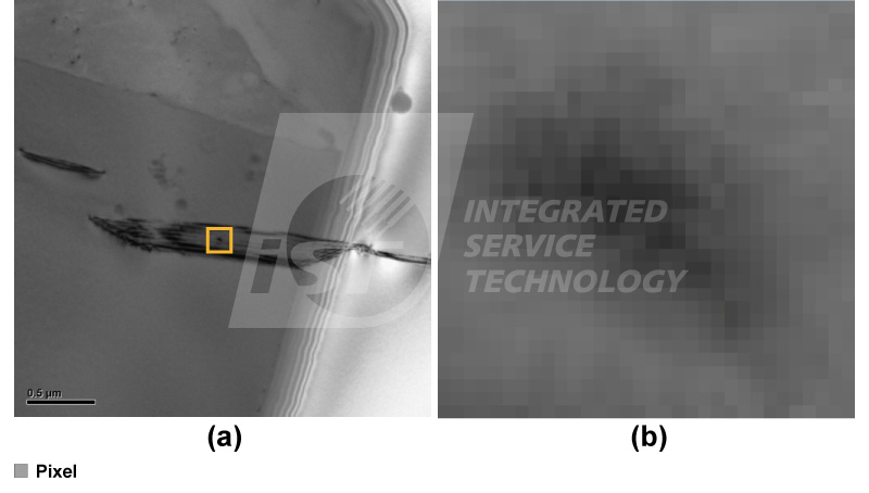
Figure 1 : A typical TEM BF (Bright Field) image and its local high magnification image. (a)A TEM BF image of Si substrate with crystal defects inside; (b)the magnified image of the yellow-framed area in image (a), pixels are visible in this high magnification image.
How Atoms in Specimen Affect the Brightness of TEM Images?
The distribution density of electrons of high energy, being emitted from the filament and passing through electro-magnetic lenses, is homogenous. If these electrons arrive the digital camera directly, the electron dose of each pixel will be almost same, then the image will have no contrast (Figure 2a), since each pixel received almost same dose of electrons. When the specimen is inserted into TEM, electrons of high energy pass through the thin foil first, then go into the digital camera. Interaction between these high-energy electrons and atoms of the specimen modifies the distribution density of incident electrons. Thus, the distribution density of incident electrons is no longer homogeneous. It means that each pixel of digital camera accepts different electron dose and displays different grey level, pixels of higher dose show brighter grey levels and pixels of lower dose show darker grey levels (Figure 2b). This makes TEM images have brightness contrast. Following, we will discuss how atoms in the specimen modify the distribution density of incident electrons.
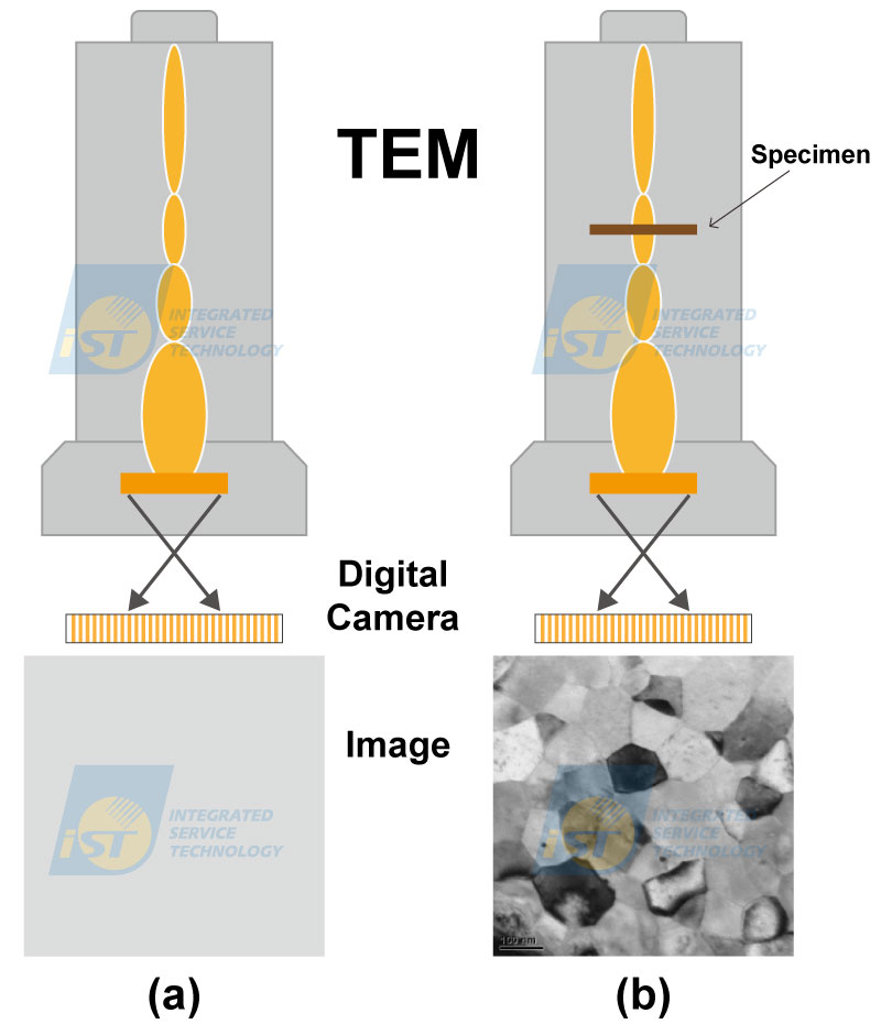
Figure 2 : Schematic diagram shows the effect of a TEM specimen on the brightness of pixels. (a) without specimen, (b) with specimen.
Multi-physiognomy of TEM images
Contrast of features in TEM images tells material information in the specimen. However, the contrast of features in TEM images is not unique. The contrast and the morphology of features change with TEM operation conditions and the operating mode. Figure 3 shows a typical case. The contrast and morphology of dislocations marked A and B are different in three images. Are these dislocations single line type? or two lines close to each other? or three lines close to each other? If the number of dislocations is related to the condition of heat treatment, misjudging the number of dislocations will lead to wrong direction of process tuning. This would result in a waste of time, human power, and material resource. On the contrary, if R&D engineers and/or process engineers received correct TEM images, quickly and correctly interpreted information inside, and developed a right direction of process tuning, they will increase company’s income.
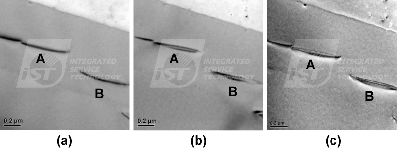
Figure 3 : The morphology and contrast of dislocations A and B vary in three TEM BF images which recorded at different specimen tilting conditions.
Nothing but Scattering and/or Diffraction
At the first glance, the variation of brightness of TEM images seems very complicated. Briefly, they can be categorized into two contrast mechanisms, scattering and diffraction. Scattering is that the trajectories of incident electrons are deflected by nuclei of elements which consist of the analyzed materials. Electrons scattered to high angles, which are out of the range of the detector, don’t contribute to the image. The larger atomic number of the element, the higher charge the nucleus carries, and more incident electrons are scattered out of the detector. This results in dark contrast for regions consisted of heavy elements (Figure 4a). The image contrast increases when an object (OBJ) aperture is inserted. For regions consisted of elements of close atomic numbers, those of higher density have more significant scattering effect and show darker contrast, as interpreted by Figure 5.
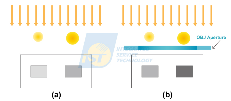
Figure 4 : Effect of atom number of the elements on the brightness of TEM images. (a)before an OBJ aperture inserted, (b)after an OBJ aperture inserted. The OBJ aperture blocks off some electrons to form the image, regions consisted of heavier atoms become darker due to more electrons being blocked off. (a large disc stands for large atomic number)
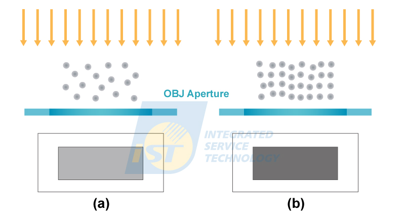
Figure 5 : The effect of density of atoms on image contrast. (a)low density, (b)high density. TEM images of regions with higher density of atoms are darker due to more incident electrons are blocked by the OBJ aperture.
Solid state materials can be divided into two groups, amorphous and crystalline. For amorphous materials, contrast of TEM BF images is dominated by scattering effect. In TEM images of semiconductor devices, amorphous silicon nitride is always obviously darker than amorphous silicon oxide (Figure 6). This kind of images tell that the density of silicon nitride is significantly higher than that of silicon oxide. In other words, the structure of amorphous silicon nitride is much denser. That’s why amorphous silicon nitride is used as passivation layers to protect transistors and the whole chip from invasion of vapor.
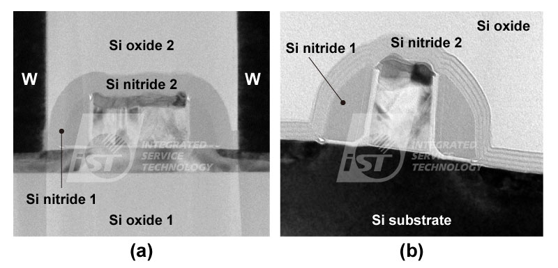
Figure 6 : Typical TEM BF image of metal oxide semiconductor (MOS) devices. W plugs and Si substrate are dark, poly silicon and metal silicide show variation contrast, amorphous silicon oxide is always brighter than amorphous silicon nitride.
Apart from the scattering contrast, crystalline materials have diffraction contrast in TEM BF images. When the angle of some crystal planes and incident beam approaches a Bragg diffraction angle, such as exact zone or two beam condition, these grains will become dark due to some diffraction beams being blocked off by the objective aperture and not contributing to the image, thus, pixels of these grains receive less electrons and show dark contrast.
Similar Brightness but not Same Phase? How to Avoid Causing Panic Due to Misjudgment?
During TEM observations, tilting the specimen will change the angle between some groups of crystal planes and the incident beam, and diffraction conditions of those crystal planes change at the same time. In TEM BF images of semiconductor devices, the brightness of crystalline materials, such as poly silicon, metal silicide, metal lines etc., varies with specimen tilting, but that of amorphous phases, silicon oxide and silicon nitride, keeps same at all times. W plugs are a crystalline phase but always dark due to its high atomic number. In some semiconductor devices, tungsten compound is surrounded by poly silicon. When the orientation of some Si grains is happened to be at strong diffraction conditions, and the brightness of these Si grains is very close to that of tungsten compound, as shown in figure 6.These dark Si grains are frequently misinterpreted to be tungsten diffusion by R&D engineers and process engineers who are not familiar with the mechanism of TEM image contrast, resulting in unnecessary panic. Similar incidents are frequently heard in various semiconductor factories.
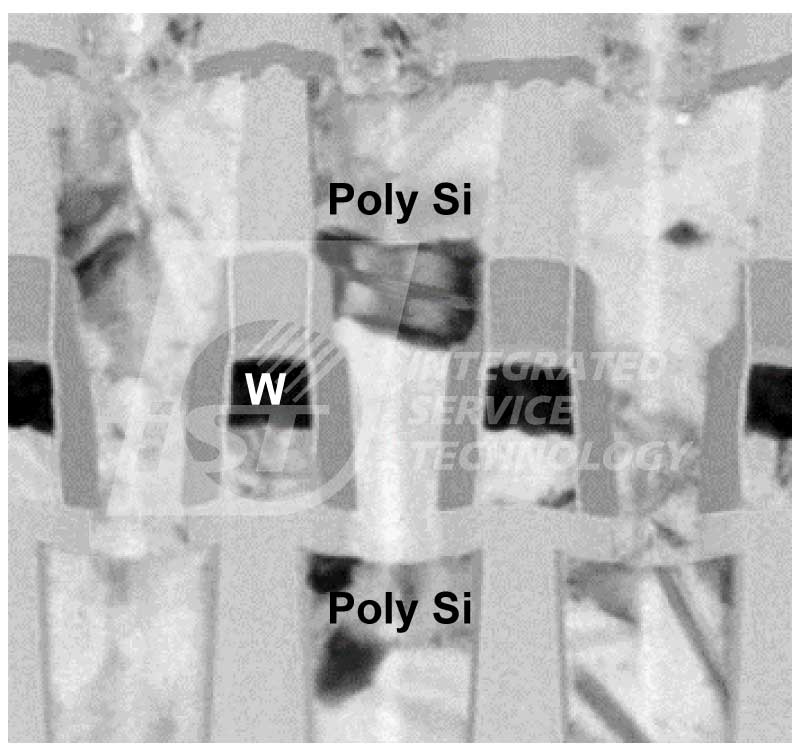
Figure 7 : TEM BF image of semiconductor device. The structure with tungsten compound (one of them is labelled “W”) inside is surrounded by poly silicon.
Familiarity with scattering and diffraction principles is essential for improving processes in semiconductor manufacturing
In summary, there are two contrast mechanisms, scattering and diffraction, for TEM BF images. Once we are familiar with their basic principles and interpret TEM images carefully. All material information in TEM BF images will be extracted to help following process tuning.
This is to share knowledge and experiences of iST with you. Should there be any inquiry or if you would like to know more about the aforementioned techniques, just email us at marketing_tw@istgroup.com。