Issued Date:2022/5/26 advanced process defect
Issued By:iST
While process equipment is the key to semiconductor yield, how to improve advanced process defect through materials analysis?
The advanced process war among TSMC, Intel and Samsung, world-leading semiconductor manufacturers, began in full swing in 2022. Although each has placed huge investments in various types of advanced process equipment, which boosted the demand for such equipment as the extreme ultraviolet (EUV) lithographic equipment wherein the yield is the key to success in this war. While there is a good many factors affecting yields, the iST Classroom will focus on two topics: How do advanced process defect affect yields? How to improve defects through materials analysis?
advanced process defect

1. How does process equipment affect IC yields?
Following the cost change and technological advancement in the integrated circuit (IC) process, wafer sizes have quickly been switched from 4 inches, 6 inches, 8 inches to 12 inches steadily and the yield has always been the key indicator for effective IC chip count.
After repeated use in the manufacturing process, the vacuum chamber and internal parts of process equipment (e.g., photolithography, etching, wet cleaning, coating and even loading and delivery equipment…) will be contaminated or byproduct deposits will affect IC yields. Hence, periodic maintenance (PM) or part replacement is required.
In addition, while component circuits are also miniaturized to the nanoscale according to the Moore’s Law, process byproducts (or contamination) are (is) unbearable. Hence, besides increasing the PM frequency, continuous improvement of related equipment parts is required to reduce particle production and thereby enhance the yield rate.
2. Mask contamination: Cause of EUV lithography defects
Currently, the photolithographic equipment is the major influence on the yield of nanoscale advanced processes. For example, if there is one particle on the mask used in the EUV lithographer, fixed defects will be found on all chips of the entire piece of wafer to reduce the yield of the whole piece of wafer to “zero.” Therefore, this is an unbearable condition in the wafter manufacturing process.
To find out how this contaminant or foreign matter is produced, it is necessary to analyze the particle or defect source, observing the cross-section with the dual beam FIB or smaller defects with the transmission electron microscopy (TEM) which is the most straightforward method.
Figure 1 shows three different defect sources. The particle EDS analysis results in the upper right corner show that contamination is caused by elements including C, O and Si falling on the surface of the anti-reflection coating. The image in the lower right corner shows that defects fall on the capping layer. The image on the left shows that the etching residue on the mask right at the beginning is the cause of defects. The sources of all these defects can be determined by composition analysis with the energy dispersive spectrometer (EDS) for mask fabs to make improvement.
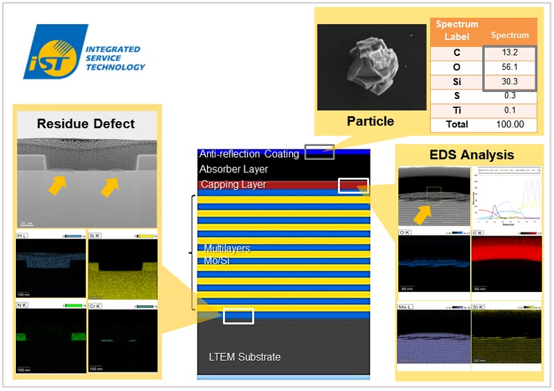
Figure 1: Cross-Sectional EDS composition analysis of mask contamination or defects.
3. How to minimize the defects caused by etching process equipment?
Etching equipment is currently one of the major factors affecting yield rate and components of the etching equipment include plasma generator electrodes, wafer trays, vacuum chamber walls and pipelines. In the reactive ion etching process, gases such as fluoride will be injected to the chamber parts to cause etching, thus these chamber parts must be replaced periodically. Besides extending the life of parts, how to reduce (or eliminate) byproduct production is also an important issue.
(1) Verifying the flatness and density of vacuum chambers and part surface coating with analysis tools
In the early times, most chamber parts were protected with SiO2 and Al2O3 surface coatings. However, particles and byproducts were produced very easily from the reaction of fluoride with SiO2 and Al2O3 and the anti-corrosion effect was not good. Later research found that although Y2O3 could improve the situation significantly, it was unable to effectively resolve particle production. In the research in recent years, new coating materials such as Y2O3 surface fluorination, YF3 and YOF, different yttrium fluoride materials have been tried in the etching durability test.
In related research, the requirements for surface coating property include porosity, roughness, flatness and either the scanning electron microscope (SEM) or atomic force microscope (AFM) can be used to observe the surface morphology and roughness. After the etching and reliability tests of the etching equipment, besides observing the changes in the surface morphology and roughness, surface byproduct formation can be analyzed and the differences before and after can be compared. Figure 2 shows the Y2O3 coating after fluoride-based plasma etching. SEM was used to observe the surface morphology and AFM was used to analyze the roughness difference before and after etching. The AFM roughness analysis shows that the roughness after etching (Rms) increased from 10.7nm to 6.5nm.
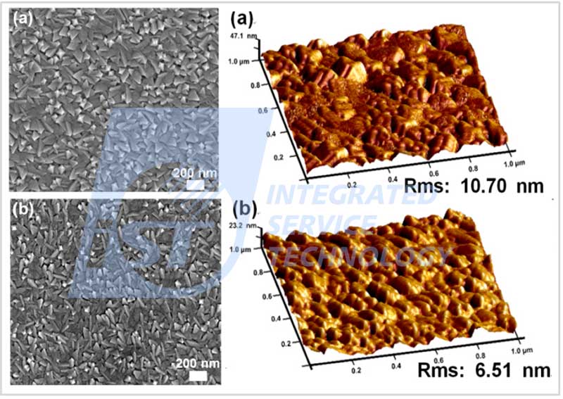
Figure 2: Surface morphology changes and roughness difference of Y2O3 coating before (a) and after (b) etching using SEM and AFM.
(Coatings 2020, 10, 637 Wei-Kai Wang, etc.)In addition, coating development research found that x-ray diffraction analysis (XRD) can be used to analyze the phase of crystallization of coating and the correlations with grain sizes. Figure 3(a) shows the crystallization characteristics of Y2O3 coating at different temperatures using XRD analysis. In addition, Figure 3(b) shows the grain size calculation using the full width at half maximum (FWHM) of diffraction peak. These show that the grain size increases as the substrate temperature rises to facilitate coating speed and quality control.
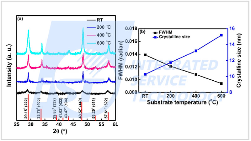
Figure 3: Correlations between crystallization characteristics and grain sizes on Y2O3 coatings at different temperatures.
(Coatings 2020, 10, 637 Wei-Kai Wang, etc.)(2) Judging coating anti-corrosion effectiveness through composition change analysis with XPS
X-ray photoelectron spectroscopy (XPS) or electron spectroscopy for chemical analysis (ESCA) can be used to analyze the depth profile and bonding of the compositional changes at dozens of nanometers deep beneath the coating to judge the thickness and chemical state of surface-forming byproducts and the anti-corrosion characteristics of materials. Figures 4(a) and 4(b) show the results of XPS depth profile analysis of Al2O3 and Y2O3 coatings, respectively, after fluoride-based plasma etching. It is clear that the surface fluoride content increases on the Y2O3 coating, forming a thicker layer of fluoride byproducts.
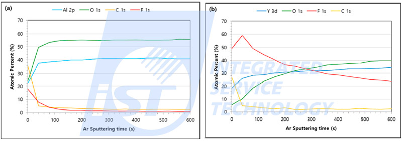
Figure 4 :Results of XPS depth profile analysis of Al2O3 and Y2O3 coatings after fluoride-based plasma etching
(Coatings 2020, 10, 1023 Seungjun Lee, etc.)In addition, high-resolution XPA/ESCA can also be used to accurately analyze the chemical state of bonding of this layer of byproducts. Figures 5(a) and 5(b) show the chemical state of bonding of the Al2p energy spectrum of Al2O3 coating and Y3d energy spectrum of Y2O3 coating, respectively. These results show that chemical bonding including Al-F, Al-O and Y-F, Y-O are formed on the surface after fluoride-containing plasma etching. Apparently, the area of Y-F bonding (area under the red dotted line) contained in the Y2O3 coating is larger than that of the Y-O bonding (area under the green dotted line) which is contained in the Al2O3 coating.
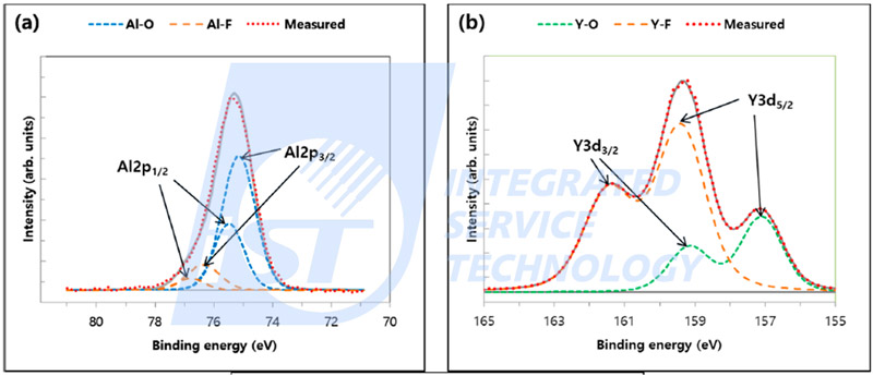
Figure 5 :High-resolution XPS analysis of the chemical state of Al2p and Y3d surface bonding on Al2O3(a) and Y2O3(b) coatings after fluoride-containing plasma etching.
(Coatings 2020, 10, 1023 Seungjun Lee, etc.)(3) Thickness and compositional analysis of coating surface byproducts
To analyze the thickness and composition of byproduct layers more accurately, high-resolution micro area observation and analysis using TEM and EDS are required. Figure 6 shows the cross-sectional TEM micro area observation of the Y2O3 coating after SF6 plasma surface processing. The left image shows that surface density increased after SF6 plasma surface processing, suggesting that this layer will provide the best protection against the subsequent fluoride-containing plasma etching. Hence, the research of related coating technology is in full swing in the latest anti-corrosion materials YOF.
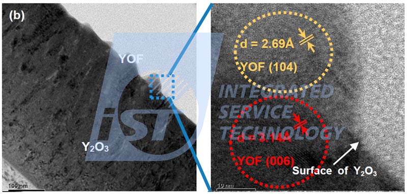
Figure 6: Cross-Sectional TEM observation of Y2O3 coating after SF6 plasma surface processing.
(Coatings 2020, 10, 637 Wei-Kai Wang, etc.)4. Total CMP process defect exposure with AFM
In addition, the chemical-mechanical polishing (CMP) in the back-end processes also affect the product yield rate. When the metal and di-electric layer becomes thinner and circuit density increases, uneven CMP will take place more easily to form residues, causing anomalies such as circuit leakage.
Hence, residue or particle formation should be noticed in the CMP. In general, AFM is used to analyze etching changes or residue marks before and after CMP for the reference of subsequent improvement. Figure 7 shows the changes before and after CMP of high-density copper circuit observed by AFM. Besides analyzing the etching rate, AFM allows the observation of particles and residues formed by CMP. The results become important indicators for adjusting CMP parameters.
As shown above, there are different types of materials analysis tools for equipment used in different processes. They all aim to find out the most suitable and most durable materials to ensure zero defects for advanced processes.
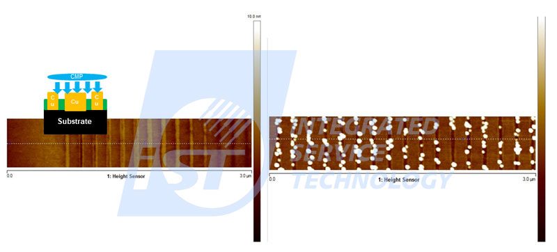
Figure 7 :AFM analysis results of copper circuits before (left) and after (right) CMP.
The size of the coupons for analyzing the parts of the above equipment is usually 10-20mm for use in the vacuum analysis equipment (e.g., SEM, DB-FIB) for observation and analysis. At iST, the materials analysis lab can run the DB-FIB test, cross-section, sampling and compositional analysis for mast coupons at or below 6 inches. In addition, through collaboration with external contractors, the materials analysis lab also provides SEM analysis service for parts of large chambers at 12 inches without additional broken chips for direct tests and EDS analysis at the same time.
In case you have any needs or want to learn more about what it is all about, please contact us at +886-3-579-9909 Ext. 6613 Chiru Chang or Ext.6161 Jay Wang│ Email: web_ma@istgroup.com;marketing_tw@istgroup.com
Other services you may be interested in
advanced process defect