
Issued Date:2026/10/29
Issued By:iST
Power semiconductors are advancing rapidly. As IGBT power modules become more complex and operate at higher power densities, an IGBT defect can be difficult to locate when thick metal layers and substrates block optical access. How can backside analysis help pinpoint the failure site?
The expansion of AI data centers, electric vehicles, energy storage systems, and power grid equipment continues to drive demand for power semiconductors. As IGBT modules become more complex, locating an IGBT defect becomes increasingly challenging: electrical measurements may reveal an abnormality, while metal layers and thermal structures obscure the failure site.
From industrial motor drives and electric vehicle traction inverters to renewable energy power conversion, IGBTs remain essential components in high-power applications. Advances in die, packaging, and thermal design continue to increase their power density. However, integrating multiple dies and material layers into a module also complicates failure analysis. When these structures block optical access, how can the defect be located?
In this edition of iST Classroom, we introduce the iST Failure Analysis (FA) Laboratory’s proprietary substrate removal techniques and electrical verification methods. From backside sample preparation and electrical verification to fault localization, we explain how backside analysis can help overcome the challenges of IGBT defect localization.
I. What Is an IGBT, and Why Is It Suitable for High-Power Applications?
An insulated gate bipolar transistor (IGBT) combines the voltage-controlled operation of a MOS structure with bipolar carrier transport. The gate voltage controls the main current flowing between the collector and emitter.
A typical IGBT has its emitter on the front side and its collector on the backside. The drift region supports high voltage, while electrons and holes conduct current together to reduce conduction losses. With high input impedance, high current density, and a low on-state voltage drop, IGBTs are well suited to high-power applications.
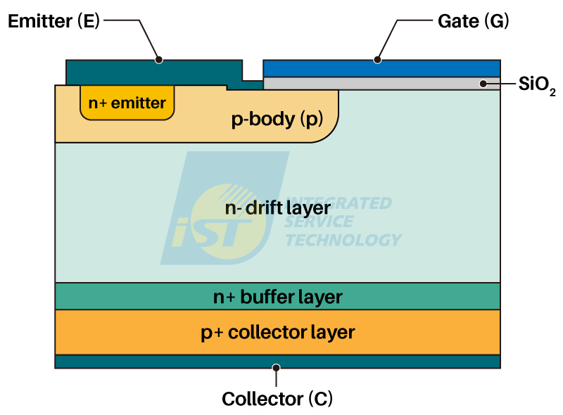
Figure 1: Schematic of a typical vertical IGBT structure.
(Source: iST)II. From Die to Module: Increasing Complexity in IGBT Failure Analysis
At the die level, technologies such as trench gates, field-stop structures, and wafer thinning continue to improve the balance among voltage blocking capability, conduction losses, and switching losses.
At the module level, active metal brazed (AMB) ceramic substrates, silver/copper sintering, copper clips, and double-sided cooling are among the approaches used to improve module performance. However, these structural improvements also affect electrical measurements, fault localization, and sample preparation during failure analysis. Understanding the module’s internal layout is therefore essential to selecting the right methods for IGBT defect localization.
III. Three Key Challenges in IGBT Module Fault Localization: Metal Shielding, Heat Spreading, and Sample Preparation Risks
In addition to the dies, an IGBT module contains die-attach layers, power substrates, metal interconnects, and encapsulation materials. Some products also include a copper baseplate for heat dissipation. These structures support electrical conduction, insulation, and thermal management, but they also make internal defects harder to observe.
When a module exhibits leakage, such as abnormal ICES or IGES, or a short circuit, front-side inspection can first identify visible damage, including wire lift-off or package rupture. However, defects within the die often present the following three challenges:
(1) Metal shielding:
Large-area emitter metallization and thick copper clips on the die’s front side may block laser or infrared optical access. This can prevent tools such as OBIRCH and InGaAs emission microscopy from detecting signals from the underlying MOS gate structures and channels.
(2) Heat spreading:
The highly thermally conductive top metallization can spread localized heat outward, broadening the apparent hot spot and making it difficult to obtain precise coordinates for subsequent cross-sectional analysis.
(3) Sample preparation damage:
The module may be filled with silicone gel or epoxy resin. Improper decapsulation or encapsulant removal can break bond wires or corrode metal, altering the original failure characteristics.
When front-side observation is limited, backside analysis may offer an alternative approach to IGBT defect localization. However, baseplates, die-attach layers, ceramic substrates, and metal layers may also obstruct backside access and must first be removed.
The key is to remove these obstructing materials uniformly while verifying that the original electrical abnormality can still be reproduced. This establishes the conditions required for subsequent backside observation and fault localization.
IV. iST’s Proprietary Substrate Removal Techniques: Improving Failure Analysis Success Through Backside Access
The following six steps explain how the iST FA Laboratory combines proprietary sample preparation techniques with electrical verification and fault localization to trace a module-level abnormality to an IGBT defect within the die.
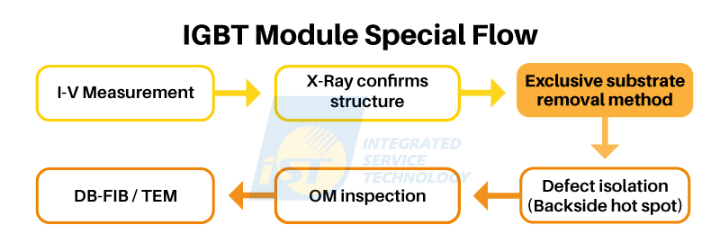
Figure 2: The iST FA Laboratory uses proprietary techniques to locate failure sites in IGBT dies.
(Source: iST)Step 1: Verify Electrical Characteristics and Narrow Down the Suspect Area
Electrical measurements first establish the IGBT die’s failure signature, such as a short circuit, leakage, or high resistance. The module circuit and terminal configuration are then used to narrow down the affected phase and suspect dies.
When multiple dies are connected in parallel, structural information and fault localization techniques are needed to distinguish among them and further identify the source of the abnormality.
Want to identify which phase of an IGBT module is faulty? Email us to request the “IGBT Module Three-Phase Fault Detection: Pinout and Measurement Point Quick Reference”—a single diagram providing a quick reference to module terminals and measurement points.
Step 2: Remove Substrate Structures Using iST’s Proprietary Techniques to Expose the Die Backside
Beneath the dies, an IGBT module may contain die-attach layers, power substrates, and a thermal baseplate. iST develops a removal process tailored to the module structure and uses customized chemical reagents to remove the relevant materials uniformly, exposing the die backside.
Step 3: Compare Electrical Results and Infrared Images to Assess Sample Preparation
After processing, electrical measurements confirm whether the original abnormality remains. An infrared optical microscope (IROM) is then used to inspect the die backside.
If the image is unclear, factors such as residual metal, silicon thickness, and surface condition are evaluated. Additional processing is performed as needed to establish suitable optical access for backside analysis.
Step 4: Perform Further Demetallization and Final Electrical Verification
A second chemical treatment using customized reagents removes residual metal films. The IGBT die’s electrical characteristics and infrared images are then checked again.
At this stage, backside optical microscopy can provide further observation of die backside structures and suspected abnormal regions. The features that can be observed depend on the device design.
Step 5: Select Tools Based on Signal Characteristics to Locate Suspected Failure Sites
Based on the electrical failure mode, DC bias is applied and suitable hot spot fault localization tools are used. These include optical beam induced resistance change (OBIRCH), thermal emission microscopy (Thermal EMMI), and indium gallium arsenide (InGaAs) emission microscopy, as summarized in Table 1.
OBIRCH detects laser-induced electrical changes. Thermal EMMI and InGaAs emission microscopy capture thermal signals and photon emission, respectively.
These tools identify suspected hot spot locations to guide subsequent backside DB-FIB cross-sectioning or TEM analysis, helping pinpoint the defect. Their applicability depends on the failure mode, electrical conditions, optical transmission through the sample, and the presence of a detectable hot spot.
Table 1. Applications of electrical fault localization tools
Tool OBIRCH Thermal EMMI InGaAs Target structures Transistors / metal layers Metal layers / packages / printed circuit boards Transistors / metal layers Failure modes Leakage, short circuits, high resistance Leakage, short circuits, high resistance Leakage, short circuits, functional failures 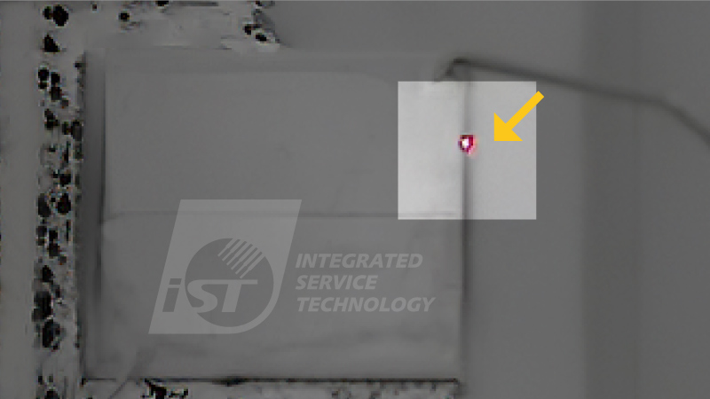
Figure 3: Thermal EMMI image showing a localized hot spot in the upper region.
(Source: iST)Step 6: Perform Localized Backside DB-FIB Cross-Sectioning and TEM Analysis for Further Confirmation
Whether a suspected defect is identified through optical microscopy or a hot spot has been precisely localized, the next step can involve localized backside cross-sectioning using a dual-beam focused ion beam (DB-FIB) system.If needed, a specimen is then prepared for transmission electron microscopy (TEM). TEM provides nanoscale structural and materials analysis to further clarify the cause of failure.
V. After Locating a Hot Spot, We Still Need to Understand Why It Occurs
A hot spot provides a valuable lead in IGBT defect analysis, but it does not directly establish the cause of failure. Heat or photon emission may be directly associated with a defect, or it may be a secondary effect of an abnormal current path. Structural and electrical evidence must therefore be evaluated together.
Comparisons with known-good devices, along with information about failure conditions and operating history, can help clarify the relationship between the defect and the observed abnormality. From detecting an abnormality at the module terminals to confirming a defect inside the die, each stage influences the next analytical decision.
iST combines electrical verification, customized substrate removal, backside preparation, hot spot localization, and DB-FIB/TEM analysis to support IGBT defect analysis from the module level to the die level.
This workflow helps customers quickly narrow down the suspect area, locate failure sites, and identify the actual failure mechanism, accelerating product validation and yield improvement for automotive-grade and high-power products.
We are pleased to share this experience with everyone who has supported iST over the years. Want to identify which phase of an IGBT module is faulty? Email us to request the “IGBT Module Three-Phase Fault Detection: Pinout and Measurement Point Quick Reference”, a single diagram providing a quick reference to module terminals and measurement points.
For inquiries, please contact Ms. Chen at +886-3-579-9909, ext. 1065, or email marketing_tw@istgroup.com. We will connect you with the right technical team to answer your questions.