Most of us tend to confuse the Preconditioning Test required by customer with MSL Test – what’s the difference between the two?

The schedule of low-volume engineering samples has been delayed. How can I get the IC assembly resources to proceed on schedule?….

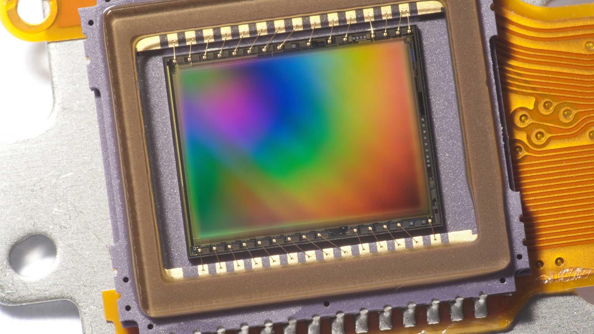
Do you ever feel helpless over the defects on CIS chips with its thinner die and 3D stacking structure…

This article is to show how to use TEM techniques to characterize the morphology, crystal structure, and composition of these gallium oxides..

Why need to use conformal coating for industrial, automotive and outdoor electronics? Why does sulfur corrosion failure still occurred on electronics with conformal coating? How to choose the correct coating material through S-corrosion verification platform..

How to perform precise electrical characteristics measurement and defect localization on those interested transistors, which are only a few nanometers in size, poses a great challenge in recent semiconductor development…
