TEM DF, the useful feature of TEM. How to select at least 8 types of TEM image analysis techniques to achieve efficient & effective material analysis?

When Si can’t meet the demands of high-speed transmission & high voltage, it’s imperative to find the best wide bandgap material to replace…

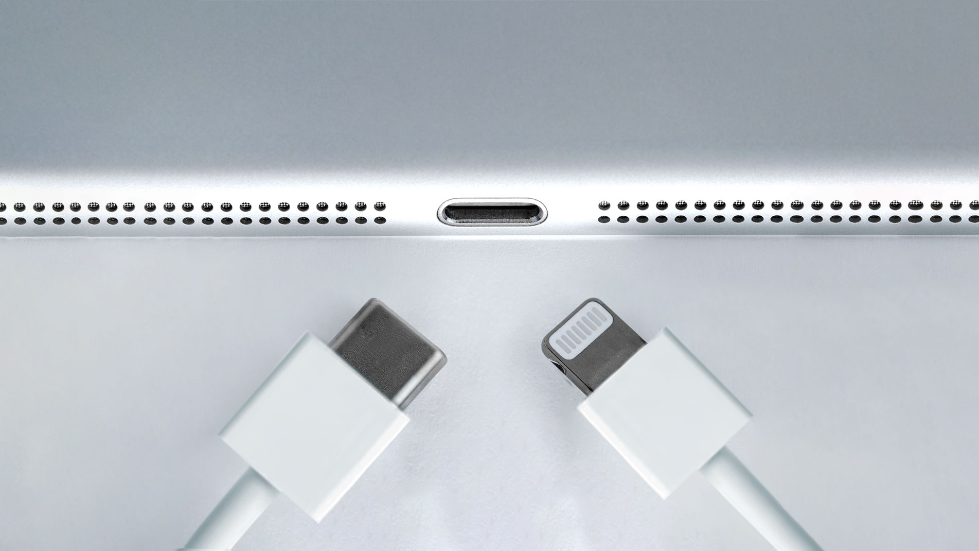
USB Type-C become the dominant standard of combining file transfer, video output & charging funtion but the compatibility issues remain a challenge…

Although it is the same TEM black and white image,there can be drastically different interpretations. What knowledge lies between the black and white of TEM images, and how to ensure that you are on the correct side?

When Moore’s Law reaches its limit, can advanced packaging be successfully developed? Master the crystal structure depends on the tool – EBSD…

Inertia thinking may enable you to become more proficient, but it may also lead us to a wrong direction in TEM sample preparation…
