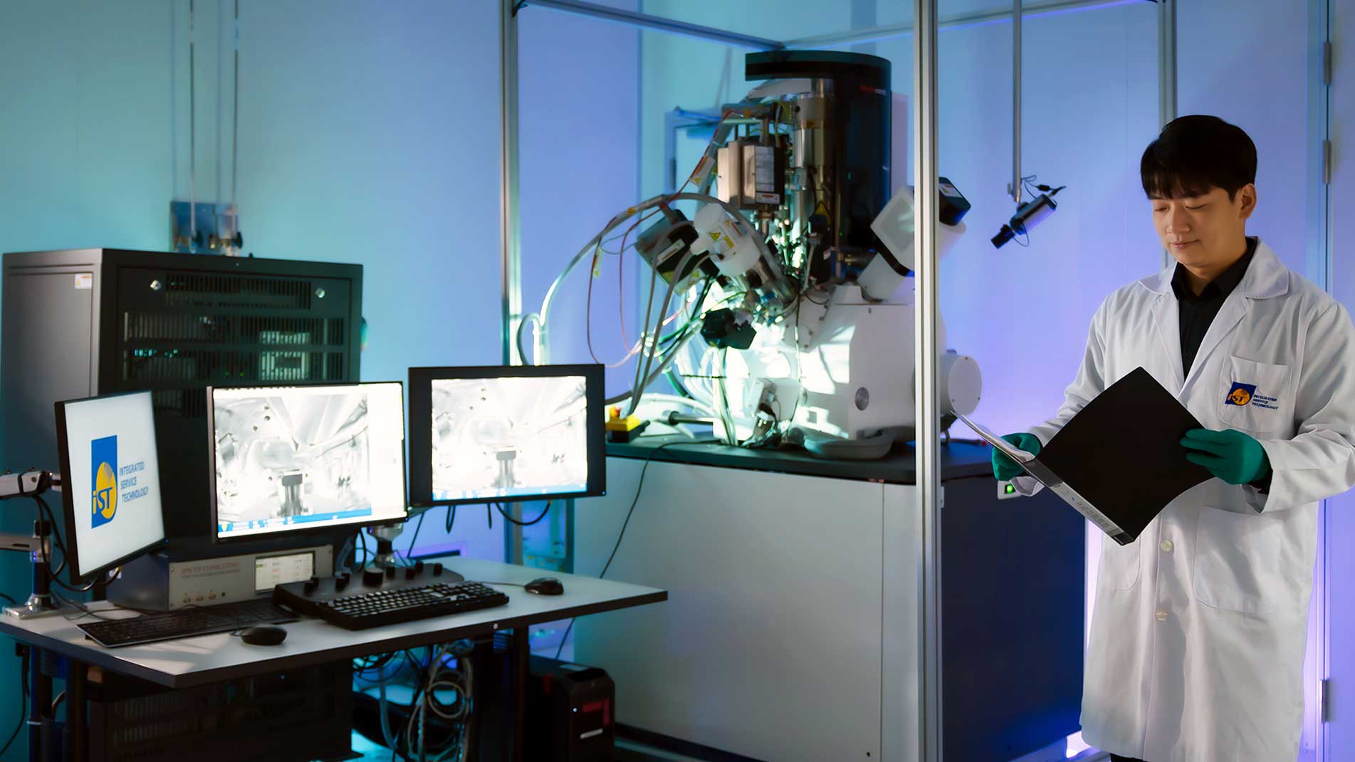
When Moore’s Law reaches its limit, can advanced packaging be successfully developed? Master the crystal structure depends on the tool – EBSD…
As we stand on the brink of this transformative shift from “electrical” to “optical,” are you ready for this revolution?

As we stand on the brink of this transformative shift from “electrical” to “optical,” are you ready for this revolution?

Thin film adhesion hardness is key to addressing the challenge of diverse material properties in advanced packaging technology. We rely on…

Thermal Analysis is an important way to understand the crucial thermal characteristics of advanced packaging materials. We’ll disclosure….

When Si can’t meet the demands of high-speed transmission & high voltage, it’s imperative to find the best wide bandgap material to replace…