Electro-less Plating process has one critical feature: it can grow NiAu or NiPdAu selectively on Al pads with a series of redox reactions instead of…

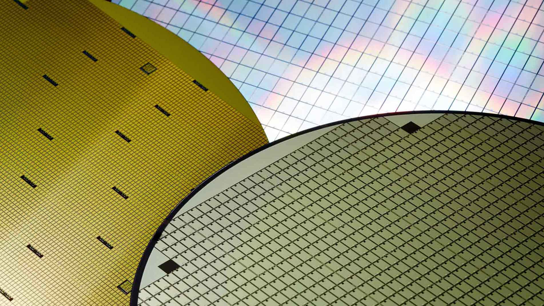
FSM is a critical process for MOSFET wafer thinning. Featuring high switch speed, low input impedance and low power consumption, the MOSFET is…
You may know you can use reverse engineering to understand IC design…

Do you know what differentiates “industry spec” and “customer spec” in the automotive electronics industry? How to do tests at the smallest cost and…

Always end up with improper analysis methods and instruments when identifying IC defects? How to select the right surface analysis tools (XPS…
MOSFET has been playing the role of “switch socket” for a long time in the electronics world. Featuring a high switching speed, low input impedance and low power consumption,…