
Do you know what differentiates “industry spec” and “customer spec” in the automotive electronics industry? How to do tests at the smallest cost and…

Always end up with improper analysis methods and instruments when identifying IC defects? How to select the right surface analysis tools (XPS…

MOSFET has been playing the role of “switch socket” for a long time in the electronics world. Featuring a high switching speed, low input impedance and low power consumption,…
To address this issue, iST has developed the solution for WLCSP IC with specific etching technique. FIB circuit edit any sites covered by the bump, RDL, or organic passivation can be achieved without problems….
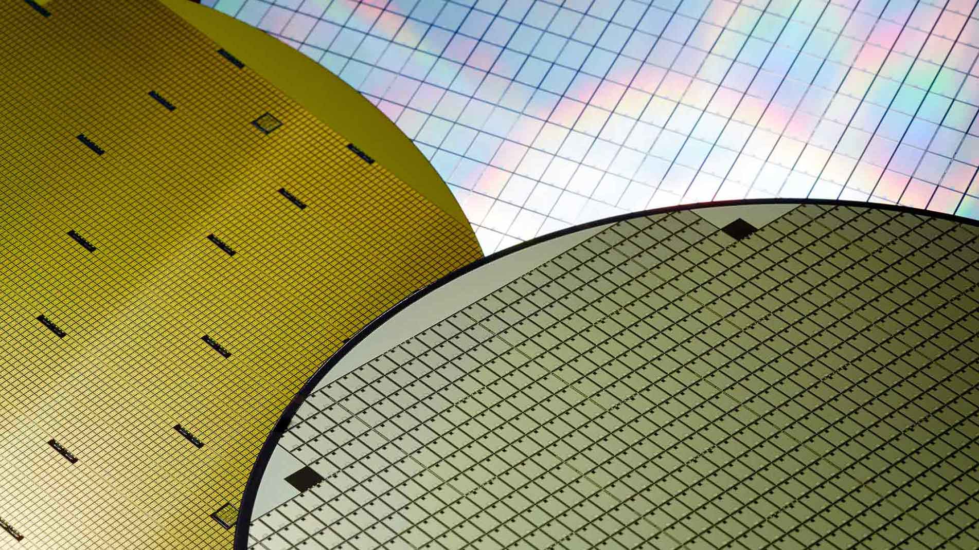
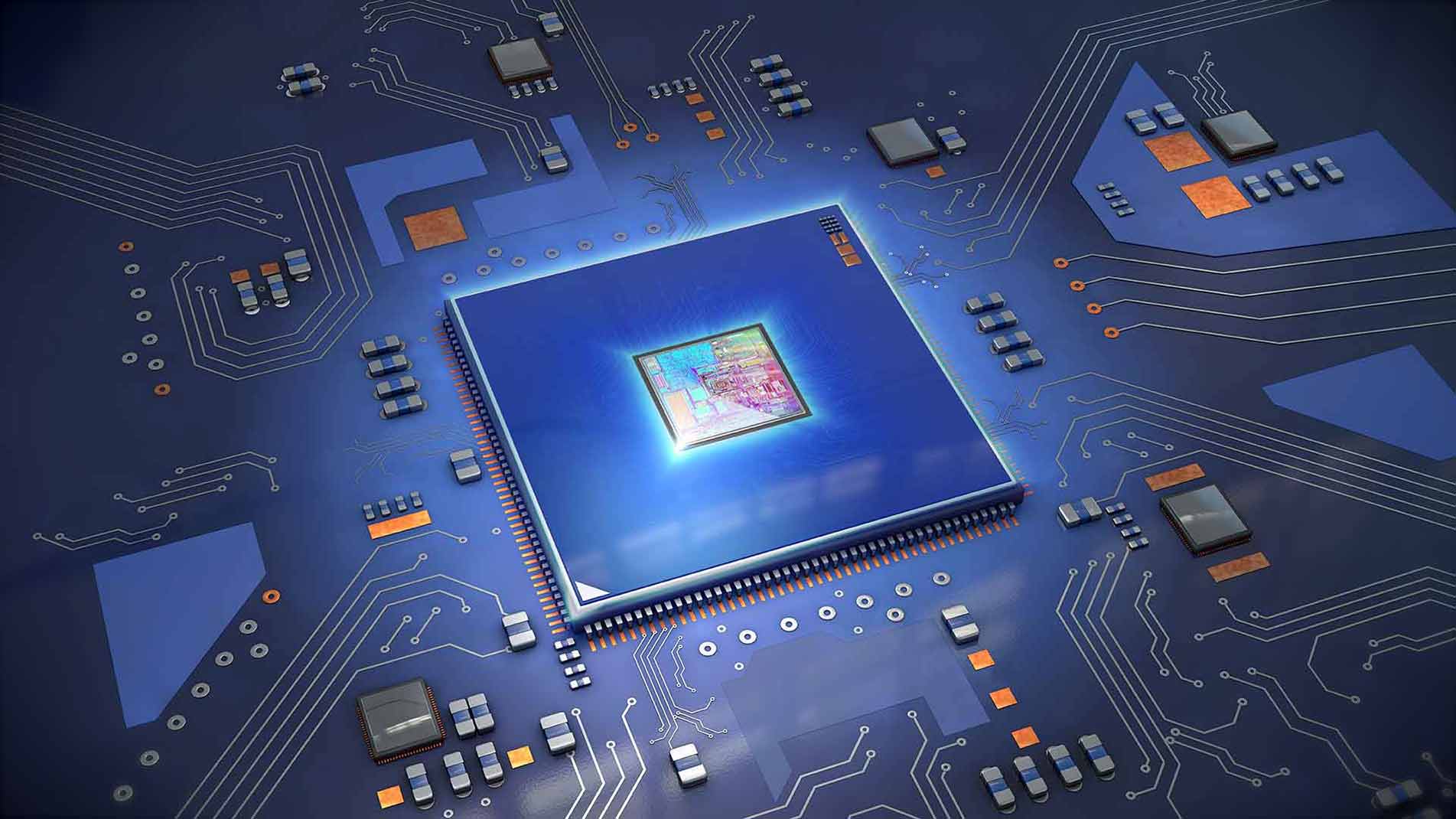
iST has decided to tap into MOSFET wafer process field, because iST has found a lack of wafer thinning and surface process available for customers between foundry and packaging operations…
What should you do to identify burnt areas in order to proceed with circuit design modification? The iST Tech Classroom presents some typical cases to help you pinpoint component EOS abnormal hot spots…