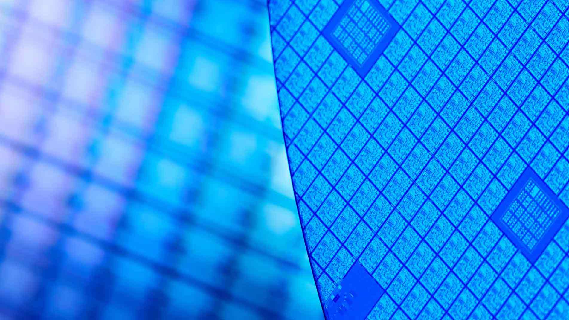
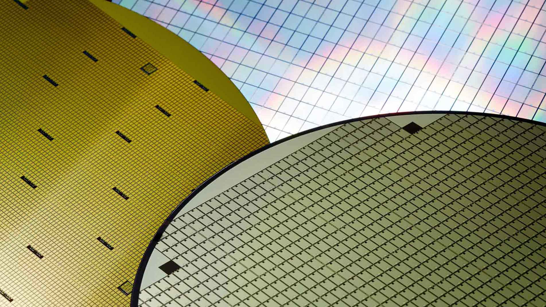
Wafer Ultra thinning has been the most direct and effective process improvement in cutting power consumption and input impedance of power semiconductors which not only reduce packaging dimension but also…
Electro-less Plating process has one critical feature: it can grow NiAu or NiPdAu selectively on Al pads with a series of redox reactions instead of…
FSM is a critical process for MOSFET wafer thinning. Featuring high switch speed, low input impedance and low power consumption, the MOSFET is…
MOSFET has been playing the role of “switch socket” for a long time in the electronics world. Featuring a high switching speed, low input impedance and low power consumption,…

iST has decided to tap into MOSFET wafer process field, because iST has found a lack of wafer thinning and surface process available for customers between foundry and packaging operations…