ICs have been evolving for faster speed, lower power consumption, and least production cost. This is reflected in process technology in three aspects:
- The first is breaking the Moore’s Law from 28nm-16nm-10nm-7nm-5nm and further down to still smaller line widths.
- The second is lifting upward from 2D (plane) structure to stack chips into 2.5D or 3D hierarchy.
- More efficient power conversion and applications.
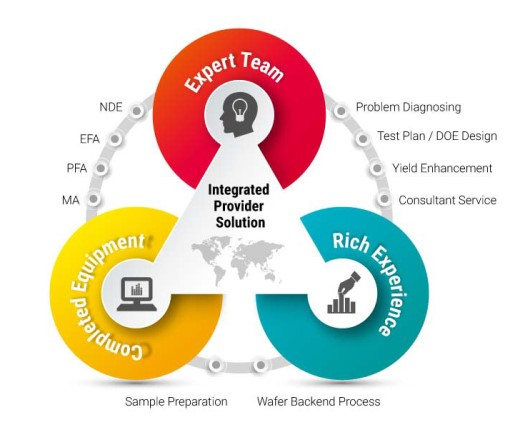
iST is ready to assist customers not only in dealing with product failures, but assists customers to identify product failure mode and find out root cause. Furthermore, to provide wafer backend process integrated services for component-related customers.
iST has a world class verification zone to secure your sample products from any information leaks and hacks.
Launch speed of new IC products is determined by shortening the development schedule from assessment through design to mass production. In case there is circuit modification due to defects found in early design stage, iST may provide series of services including special sample preparation , and employ advanced FIB circuit edit, then verify testing again without replacing mask process to cut mass production schedule. Regarding reliability test ,iST also provide series of experiment program including quick assembly、 SMT test sample preparation、BLR verification to control product quality.
Identify failure causes with step-by-step analysis
In case of product failure (R&D or RMA) and requiring further analysis, iST’s comprehensive failure analysis platform is always ready to serve customers with: ultra-resolution 3D X-Ray、SAT, electric characteristics measurement and analysis like IV measurement for device feature comparison; defect spot positioning like Thermal EMMI、InGaAs、OBIRCH
All these combined with complete sample pre-processing technologies including IC decap、IC delayer、cross-section & backside grinding、ion beam cross-section polishing (CP) along with high-resolution observation tools like field emission scanning(FESEM)、dual beam FIB) may help customers to identify failure causes by step-by-step analysis.
Regarding material analysis, iST is capable of material micro structure analysis and nano-level surface ingredient analysis including Auger Electron Spectroscopy (AES) 、X-ray electron spectroscopy (XPS) 、transmission electron microscope (TEM) 、secondary ion spectroscopy (SIMS) as well as EDS and EELS ingredient analysis to meet material analysis requirements by customer.
For power IC, iST also provides integrated backend process services through its subsidiary ProPowertek. This allows customers’ wafers to proceed directly to ProPowertek for various processes after leaving the frontend foundry. These processes include front-side metallization such as chemical/electro-less plating and front-side metal sputtering deposition; backside grinding processes including wafer thinning, taiko grinding, and backside metallization processes such as metal evaporation for backside metallization, thick Ag process, backside metal sputtering deposition, and electro-plating. Additionally, ProPowertek provides subsequent chip testing, laser marking, and die sawing services. Through comprehensive one-stop services, iST assists customers in completing various process steps from wafers to chips.
Another goal aimed for by enterprises in implementing advanced IC process is to enter into the global electronics brands’ supply chain which mandates not only high product specification but also quality management, environment protection management and CSR. iST also meets these ends with its value-added services in total quality management(IATF 16949)、environment safety and health and CSR、and greenhouse gas water footprint tracking