“TIM(Thermal Interface Materials)” has been the key to the useful life of high-power advanced packaging products which, in turn, is determined by its…

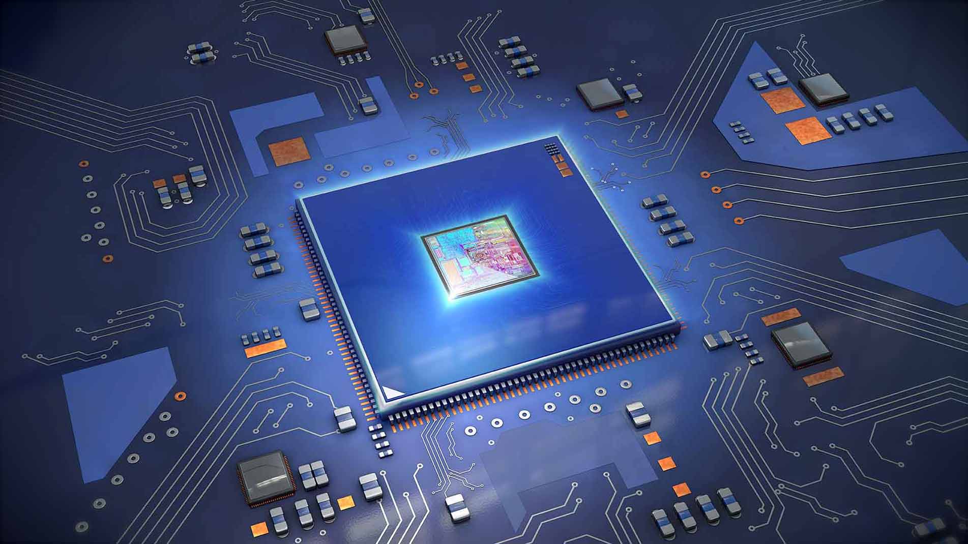
To identify failure of the single component which results in defective IC is a tall order. Internal wiring and board circuit connections among SiP, MCM, MCP, and QFP tends to suffer in electric tests by interference of other chips or device components which, in turn, makes test results hard or even impossible clear…

What should you do to identify burnt areas in order to proceed with circuit design modification? The iST Tech Classroom presents some typical cases to help you pinpoint component EOS abnormal hot spots…

The iST Tech Classroom for this month is about finding ways to pinpoint IC package defects without damaging the sample itself. Step 1: Positioning, detect failure depth…

iST presents you a hot defect detection device in non-destructive way: 3D X-ray. This hot hardware of zero-dead angle shooting and image surrounding has solved 1023 customer cases…
iST proposes 3 steps for selecting the failure analysis tools, so that the defect can be found and the true cause of failure can be identified…