
GaN defects problem solution is here! Efficiently identify defects in high-power GaN chips with iST’s exclusive Analysis…
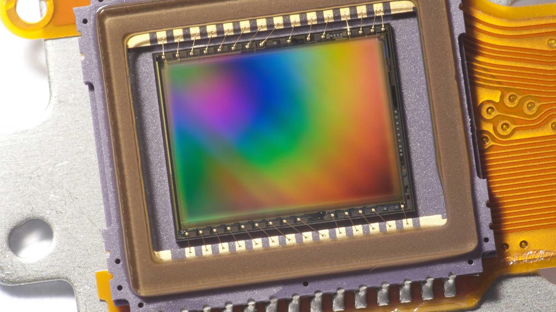
Do you ever feel helpless over the defects on CIS chips with its thinner die and 3D stacking structure…

How to perform precise electrical characteristics measurement and defect localization on those interested transistors, which are only a few nanometers in size, poses a great challenge in recent semiconductor development…

There are several methods to section a chip to solve structural issues.According to the attributes of your samples, which methodology is the best choice?…

How to quickly pinpoint defects of a FCQFN with failure analysis tools? We will show you how to pinpoint the defect position with iST‘s five steps…
Advanced packaging and heterogeneous integration is hot today. That’s the case with the quality of solder balls as well. How to identify solder ball defects quickly?