How to perform flip chip die bonding on substrate with AI pad only? How to prevent non-wetting or displacement when the copper pillar bump is replacing solder ball in the era of advanced packaging?…

Applying AI technology to the COVID-19 pandemic prevention is a hot topic now, how to apply AI in accurate pandemic prediction and prevention?

Customer requires that your product needs to meet the air quality standard of ISA 71.04 compliance for G2 or G3 level. How to face customers’ requirements…

With increasing demand in the market, GaN based III-V materials are fabricated into high brightness light emitting diode (LED) and laser diodes (LDs) [1]…

iST SMT assists you in SMT DOE tests and optimizes the combination parameters to solve SMT issues in R&D…

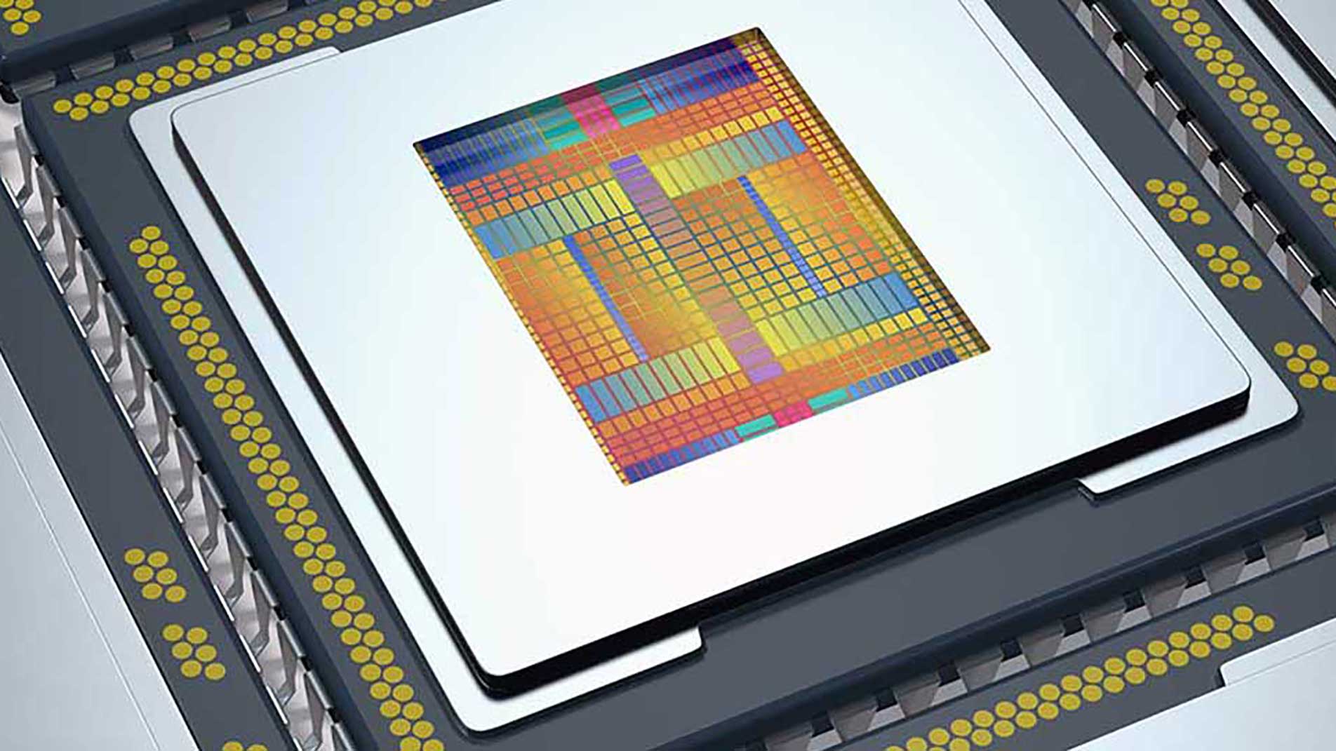
Following Moore’s Law, the industry is pushing the process to 3nm makes dies in ICs as tiny as ants’ eyes. It’s very hard to retrieve circuits…