
While process equipment is the key to semiconductor yield, how to improve advanced process defects through materials analysis?…
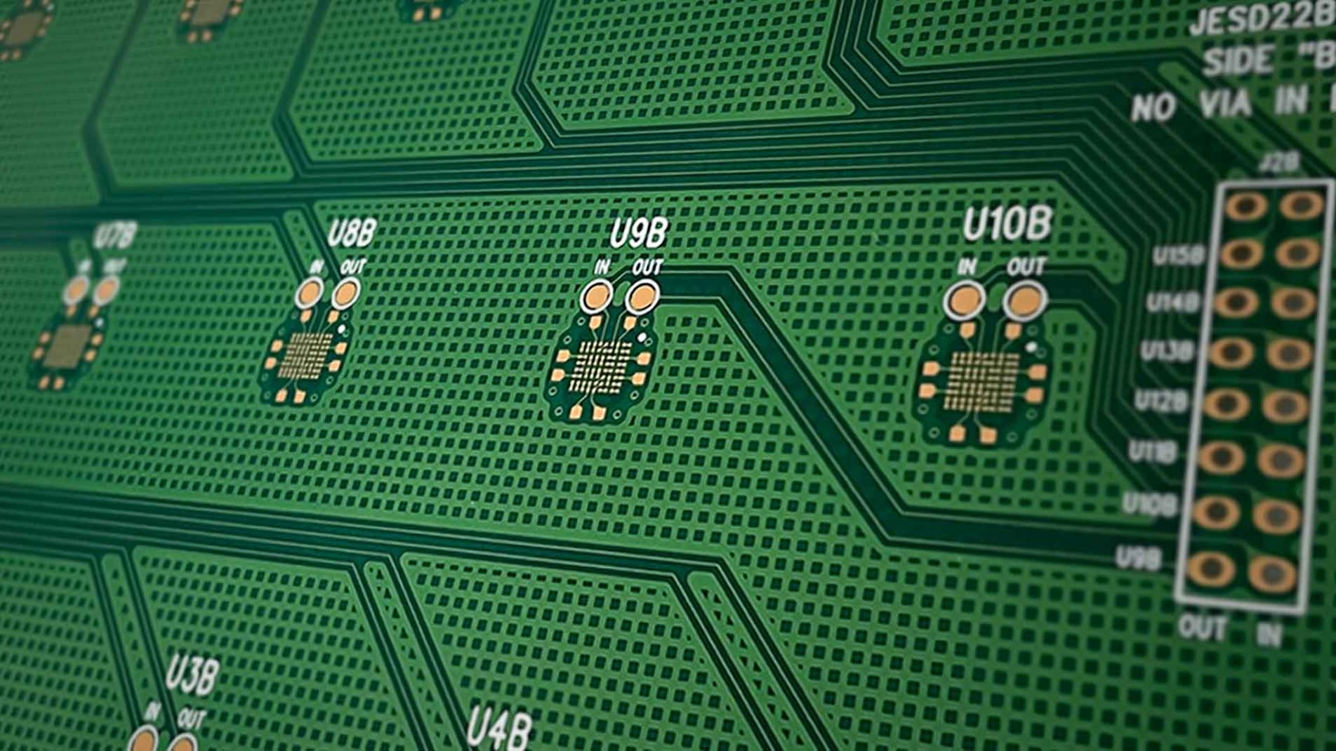
Do you know that PCB design is the key to pass or fail in broad level reliability tests?

How to interpret and use the values from HTOL and the resulting MTTF and Failure Rate (λ)? What are the differences between MTTF and MTBF?

How to find suspected defects from complicated MCP/SiP structure? How to isolate interference from other chips/dies and get correct testing results?
As an extension of grinding delayer, PFIB can perform large area and excellent uniformity delayering of a specific area or layer through plasma etching with the manufacturer’s patented gas to fully present the target area of up to 200μm x 200μm …
Have you ever wondered why your product ended up with contradicting result after ESD test by different labs? Or, shocked when two latch-up tests on the same product failed and passed respectively….