Issued Date: 2023/9/6
Issued By:Digitimes
The semiconductor manufacturing industry, which constantly pursues ultimate performance, small form factors, and minimal power consumption, has been continuously refining various technologies in recent years. Apart from the two major trends of advanced processes and compound semiconductors, advanced packaging technology for heterogeneous integration has also become a recent market focal point in conjunction with the AI popularity. However, all three of the aforementioned technologies must be accompanied by material analysis (MA) and failure analysis (FA) to ensure product quality and reliability. With ample professional experience in semiconductor analysis, Integrated Service Technology Inc. (iST) provides a variety of solutions that cater to the diverse needs of customers in this field.
Creating new technologies with professional experience to overcome analytical challenges in new production processes
Turning the attention to advanced processes, over the past two years, AI development has picked up the pace gradually. Various electronic devices and field systems have shown an increasing demand for more computing power in ICs. To meet these market demands, semiconductor manufacturers have been investing heavily in the research and development of advanced processes. Due to these efforts, the mass production of 3-nanometer chips began in the end of 2022, while the mass production of 2-nanometer chips is expected to commence in 2025. Miniaturization processes and high-density components have brought various challenges to failure analysis(FA) and material analysis(MA) in semiconductor production. Shih-Hsorng Shen, the Director of Failure Analysis Engineering Division at iST, pointed out that as component sizes decrease, internal structures become more refined. As a result, failure points will also become proportionally smaller. Analyses thus require techniques and approaches that are different from the past to address these challenges.
Demands for new analytical techniques brought forth by new processes are also created in the fields of heterogeneous integration and compound semiconductors. Shen explained that advanced processes, advanced packaging for heterogeneous integration, and compound semiconductors all give rise to fault patterns that are different from traditional processes. In traditional processes, faults typically involve issues like open circuits, short circuits, or leakage. However, new processes exhibit different faults. For example, in advanced packaging processes for heterogeneous integration that require stacking of different materials, variations in the coefficient of thermal expansion among different materials can lead to mechanical stress, impacting the overall operation of ICs. Due to diverse materials used and the intricate 3D IC architecture of heterogeneous integration, compared with inspecting a single layer in traditional 2D ICs to detect problems, diagnosing faults in 3D ICs of heterogeneous integration requires a thorough understanding of material properties, mechanical stress during fabrication, thermal effects, and layer-by-layer examination of the 3D structure to identify defect points. As a result, the difficulty level is fairly high.
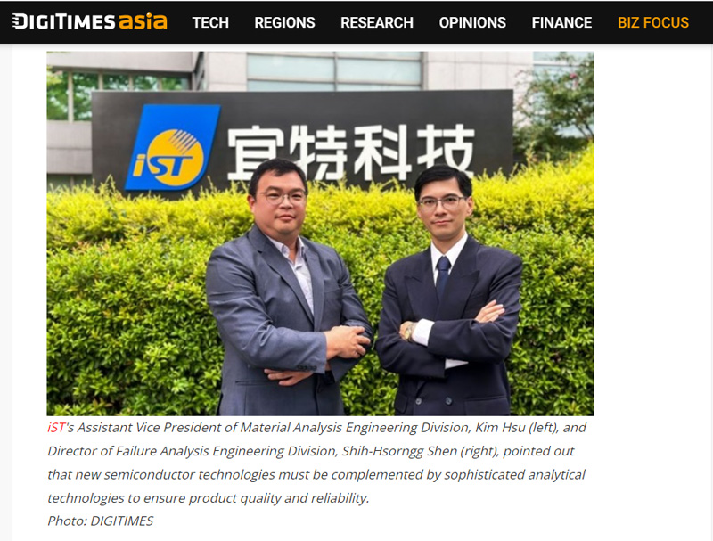
To overcome these challenges, laboratories with complete testing instruments, and extensive professional analysis experience are required. Taking thermal effects, which often lead to component failures, as an example, a thermal imager is typically used for identifying heat concentration points within the structure. If the issue still cannot be pinpointed, transmission electron microscopy (TEM) must be conducted for an in-depth microscopic material analysis. However, in the verification and analysis service industry, precision instruments only constitute the basic requirements. Kim Hsu, Assistant Vice President of Material Analysis Engineering Division at iST, pointed out that to obtain accurate results, extensive analysis experience is also essential.
Hsu further said that generally, more comprehensive information will make analysis results with higher precision. However, due to the sensitive nature of information in the semiconductor industry, clients are often less willing to provide detailed information compared with other fields. To deliver analysis results that meet client expectation despite these circumstances, different professional approaches are required.
Regarding the mechanism of semiconductor verification and analysis services, Shen used the medical field and its processes as an analogy. When a person feels unwell, he or she would usually see a family physician first. The family physician would conduct preliminary examinations such as auscultation, inspection, or use various instruments to identify the cause of illness. Once the cause is established, the patient is then referred to the appropriate specialized department, where a specialist physician would provide the corresponding treatment. iST’s verification and analysis services follow a similar approach. Shen explained that when a product fails, customers often struggle to identify the point of defect. As such, iST will first assign a single contact window to handle the case. Preliminary diagnosis will be conducted before the case is transferred to the corresponding laboratory. This practice resolves the inefficiency of past procedures, where trial and error was repeated in various analysis processes to determine the cause of defect. As a result, the time required for product analysis is significantly reduced.
Additionally, much like in hospitals, where X-rays or ultrasound scans are performed for maintaining as much integrity of a patient’s body as possible, and preventing the equipment from affecting the area under examination, verification and analysis services operate under similar principles. However, as semiconductor processes become increasingly miniaturized, the difficulty of conducting non-destructive testing has increased. iST’s unique techniques and methods often start with a pinpoint analysis for a broad area, and an elimination process layer by layer to identify the issue. Subsequently, limited-destructive or non-destructive analysis will be carried out where appropriate. The majority of the analysis work is conducted with this approach, which leads to precise results.
Consolidating years of analysis expertise to provide one-stop integrated solutions
In addition to aiding customers in swiftly identifying causes of product defects, Hsu pointed out that a product comprises an integrated structure. Therefore, failure analysis(FA) and material analysis(MA) not only have to fulfill their respective roles, but also closely interact and connect with each other to effectively ascertain the reasons for failure. During the analysis process, FA primarily focuses on identifying root causes of issues from a higher level such as mechanical and electrical causes. On the other hand, MA delves deeper into analyzing material properties to ensure that the quality and performance of materials or components align with the requirements.
Hsu continued to explain that the ability of iST in providing comprehensive solutions is underpinned by a high degree of professional expertise. He cited TEM as an example. TEM can penetrate materials to reveal their internal structures at a microscopic level. However, the results are inherently microscale. At this point, it is necessary to cross-examine and verify the microscopic results against macroscopic findings. Hence, MA and FA need to go hand in hand to identify the causes of failures.
To provide customers with the best integrated solutions, iST adopts several approaches to strengthen the capabilities of its team. Firstly, iST continues to invest in its hardware and equipment to establish a comprehensive analytical environment. Secondly, the company works to enhance the quality and quantity of its talents. Employees are encouraged to proactively participate in academic conferences, and engage in exchanges and collaborations with research institutions. Meanwhile, industry experts are also recruited into the team.
Aside from investing in hardware and cultivating talents, Shen mentioned that another important aspect is the utilization of data science in iST. He said that with the increasing data volume nowadays, data analysis and processing have become ever more important. iST uses AI-automated measurement technology to effectively reduce human error. By integrating automated measurement technology with TEM, not only can the precise dimensions, shapes, and distribution of grains and nanometer-sized particles be accurately measured, the thickness and width of thin-film layers can also be measured. Through this integration, a continuous stream of data on nanoscale components can be generated, ultimately enhancing process yield and creating new business opportunities.
In addition to advanced processes, advanced packaging for heterogeneous integration, and compound semiconductors, more new technologies will emerge in the future. In this regard, Shen said that iST will work to establish a comprehensive hardware environment, nurture cross-disciplinary talents, and develop analytical technologies. In response to the rapidly changing semiconductor industry, iST aims to become the strongest force through professional analysis services, supporting customers to emerge a winner from market competition.