Issued date: 2026/4/21
Issued by: iST
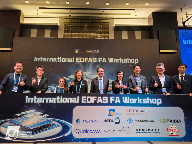
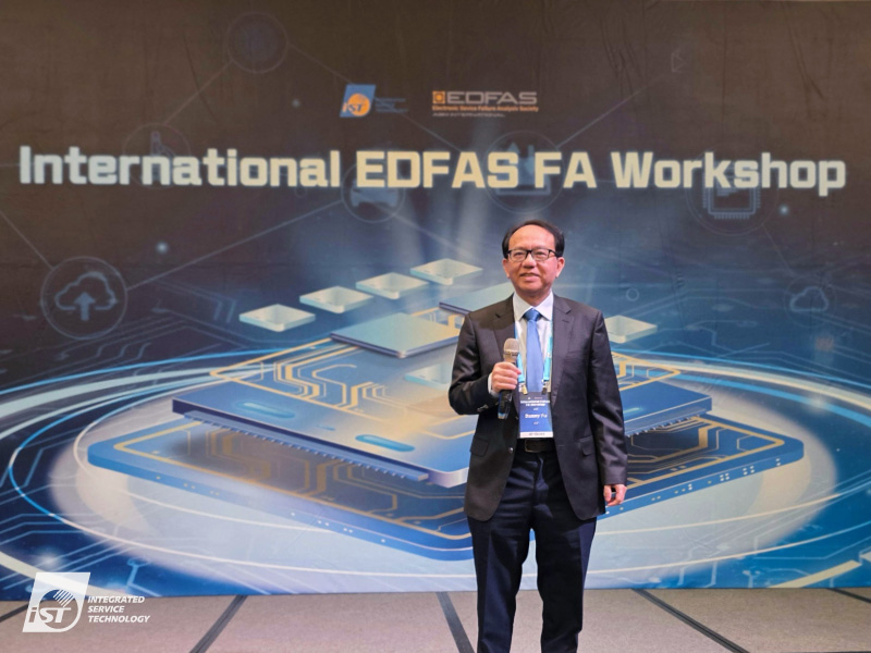
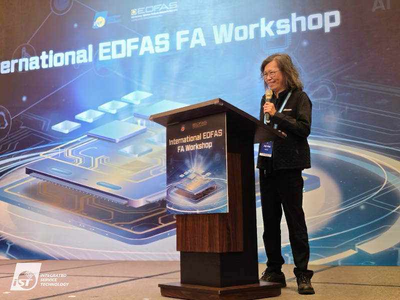
iST Chairman Danny Yu with speakers from the inaugural EDFAS Asia Workship.
iST welcomes global industry experts to Taiwan for the EDFAS FA Workshop.
iST welcomes global industry experts to Taiwan for the EDFAS FA Workshop.
iST welcomes global industry experts to Taiwan for the EDFAS FA Workshop.
iST welcomes global industry experts to Taiwan for the EDFAS FA Workshop.
iST welcomes global industry experts to Taiwan for the EDFAS FA Workshop.
iST welcomes global industry experts to Taiwan for the EDFAS FA Workshop.
iST welcomes global industry experts to Taiwan for the EDFAS FA Workshop.
iST welcomes global industry experts to Taiwan for the EDFAS FA Workshop.
iST welcomes global industry experts to Taiwan for the EDFAS FA Workshop.
iST welcomes global industry experts to Taiwan for the EDFAS FA Workshop.
iST welcomes global industry experts to Taiwan for the EDFAS FA Workshop.
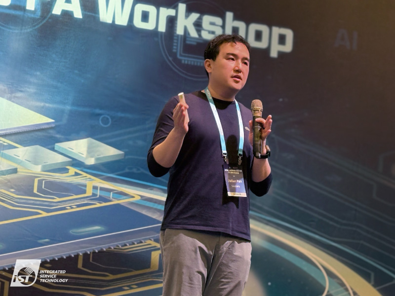
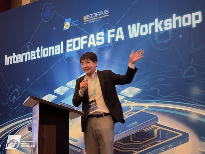
HSINCHU, TAIWAN – April 21, 2026 –The global semiconductor Failure Analysis (FA) sector has reached a historic milestone. The Electronic Device Failure Analysis Society (EDFAS), the world’s premier authority on electronic component failure analysis, has made its inaugural move into Asia this year. On April 21, 2026, EDFAS hosted a grand Failure Analysis Workshop (FA Workshop) in Hsinchu, Taiwan. As a benchmark leader in semiconductor verification and analysis in Asia, Integrated Service Technology (iST) was deeply honored to be invited as a co-organizer of this prestigious event. The Chairman of iST, Danny Yu, opened the ceremony, warmly welcoming local and international industry leaders to Taiwan.
Danny Yu emphasized that iST is deeply honored to facilitate this forum. He noted that the decision by EDFAS to hold its first-ever Asian technical workshop in Taiwan signifies Asia’s pivotal strategic position in the global semiconductor landscape. Through this platform, iST will collaborate with global experts to overcome the extreme packaging verification bottlenecks of the AI era and define new failure analysis standards for Artificial Intelligence.
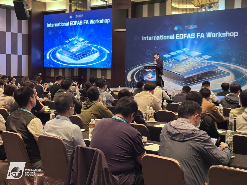
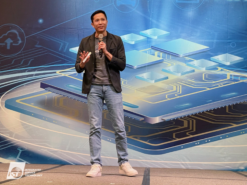
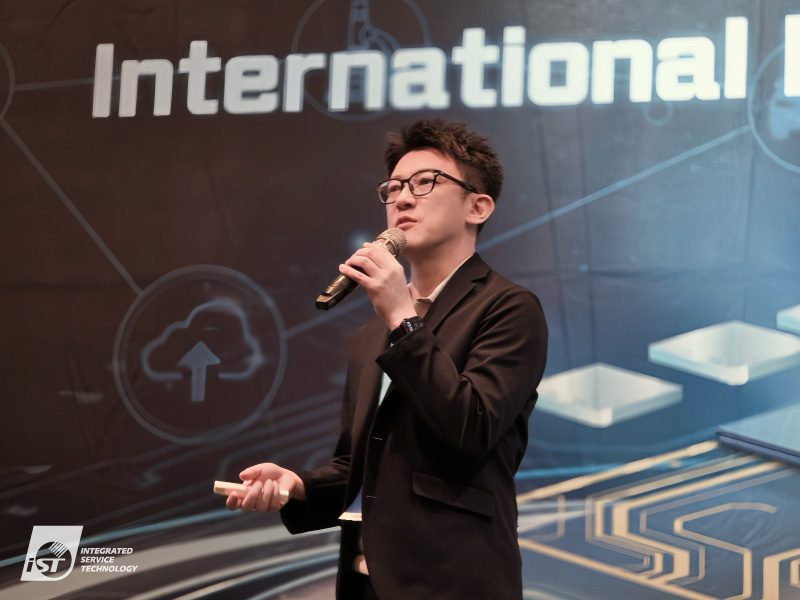
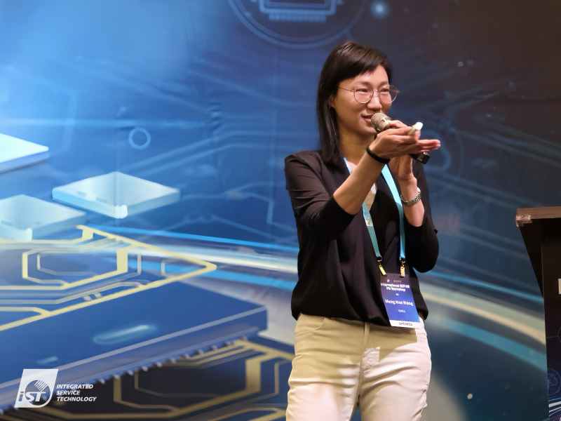
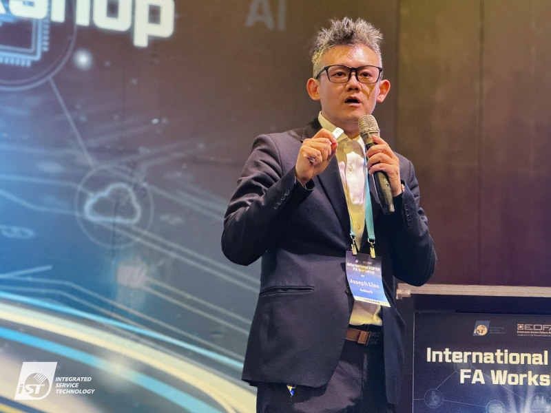
The forum saw a full house, attracting packaging and testing experts, chip designers, and R&D executives from across the globe to participate. The event gathered industry leaders such as NVIDIA, TSMC, and Qualcomm to conduct deep technical calibrations for the extremely complex packaging structures of the “Post-Generative AI Era.” As AI computing demands enter a period of explosive growth, Fault Localization within chip structures has become the ultimate hurdle in determining mass production yields and product time-to-market.
During the forum, NVIDIA unveiled its future vision for chip-level failure analysis workflows in the “Post-Generative AI Era.” With the surge in AI training and inference demands, data centers now require unprecedented high-speed transmission capabilities. NVIDIA emphasized that in high-performance and high-power environments, even microscopic signal interference or packaging defects can trigger catastrophic failures. Consequently, collaboration across design, manufacturing, system-level, and product teams from the initial design phase is essential to ensure that customers receive products with zero defects.
The mobile and computing giant Qualcomm introduced the “Data FA” data-driven analysis concept. While traditional FA typically occurs after product completion or customer returns, Qualcomm advocates for a “Shift-Left” strategy, integrating the core thinking of FA into the earliest stages of R&D. This transformation from reactive response to active defense is crucial for shortening Time-To-Market.
Meanwhile, as the global leader in semiconductor foundry services, TSMC provided a profound analysis of the practical challenges faced by Physical Failure Analysis (PFA) engineers. In addressing the complexities of advanced processes, the ability to accurately pinpoint abnormalities and trace them back to production stages under intense time-to-market pressure remains a pivotal factor in maintaining product competitiveness.
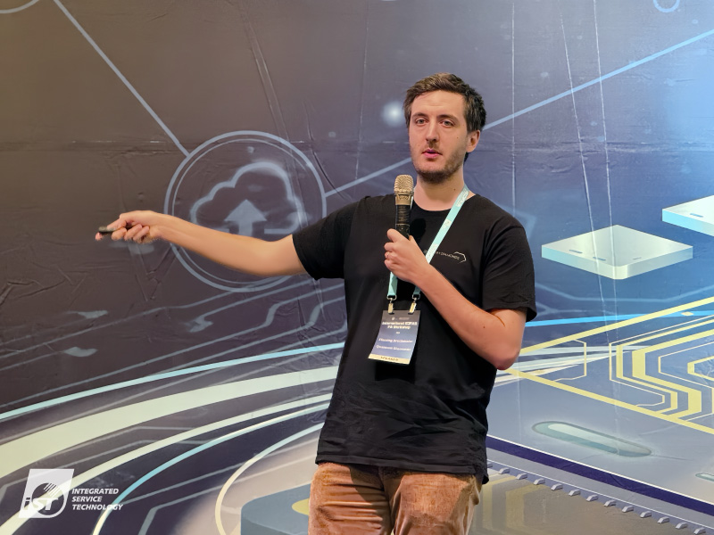
Beyond trend-sharing by industry titans, the workshop invited experts to provide diverse solutions for emerging technologies. Enlitech and SEMICAPS presented forward-looking roadmaps for Optical Loss Localization and wafer-level fault localization for Silicon Photonics and Co-Packaged Optics (CPO). Quantum Diamonds showcased the revolutionary application of Quantum Diamond Microscopy as a non-destructive inspection tool for current path imaging at the package level. Furthermore, NenoVision shared insights on Atomic Force Microscopy integrated with SEM (AFM-in-SEM), while, JEOL focused on optimization solutions for Passive Voltage Contrast (PVC) imaging, leveraging advanced sample preparation techniques to assist engineers in precisely capturing electrical defects within microscopic structures.
As a co-organizer of the EDFAS Workshop, iST showcased its advanced “Engineering Sample Preparation” and innovative “Test Interface Solutions,” demonstrating its indispensable role as a R&D backbone for industry giants. iST introduced its “From Lab to Fab: All-in-one Solution,” a comprehensive service designed to help customers complete early verification during the EVT/DVT stages. By significantly reducing design iteration costs and bridging the “final mile” before mass production, iST effectively accelerates time-to-market for its partners.
This technical summit, held for the first time in Asia, not only proves Taiwan’s core influence in the semiconductor industry but also highlights the synergy of enterprises such as iST, Enlitech, SEMICAPS, NenoVision, and JEOL. By moving in lockstep with top-tier clients like NVIDIA, TSMC, and Qualcomm, these companies continue to serve as the most powerful “unseen hands” in the Post-AI Era—precisely pinpointing fault locations, safeguarding client yields, and collectively ushering in the era of AI and Co-Packaged Optics (CPO) mass production.
About Integrated Service Technology
Founded in 1994, iST started its business with IC circuit debugging and modification and has gradually expanded its services to include Failure Analysis, Reliability Verification, Material Analysis, Signal Integrity, Chemical Analysis, and various consulting services. iST serves a broad range of customers across the electronics industry, from upstream IC design companies to downstream finished product manufacturers.
In response to emerging technological trends, iST has established comprehensive verification platforms, including Advanced Process and Advanced Packaging Verification for semiconductors, Automotive Electronics Verification, 5G/IoT/V2X/AI Verification, and Space Environment Testing Laboratories. By providing complete and all-encompassing verification and analysis services, iST continues to support its customers in addressing complex challenges in next-generation technologies.