Issued Date: 2019/3/15
Issued By: iST
Facing the IC industry’s advanced process development, iST today (Mar. 15, 2019) announced another breakthrough in IC circuit edit technology! Its backside FIB circuit editing technology can now apply to 7 nm processes, and is being recognized by advanced process customers.
iST explained the reason why the circuit editing services are required by IC design houses. It’s virtually impossible to get 100% bug-free IC design and layout, in spite of continuously improving circuit simulation software. The only way to remedy circuit defects is to modify masks, which, in turn, results in not only increasing costs but also more than one month of wait time to get new revised ICs. As a result, most IC design houses would opt for an IC circuit editing to ensure conformity of circuit design in a mere of couple of hours and much less time and cost.
iST further indicated, there are two challenges for backside circuit editing of 7 nm advanced process, firstly, is the density of transistors on wafers is up by many times: the 7 nm process technology from this year would raise density by 350% in each square millimeter over its 16 nm counterpart, let alone other greater difficulties such as, editing circuit when transistors that are all over the bottom layer.
Secondly, the thinner and smaller gap: the width, thickness and gap between dielectric layers and metals of 7 nm advanced processes, almost goes down to 40 nm or less. The largest challenge of facing thinner and smaller process technology is to position targets accurately, identify circuits clearly and prevent metal layer over-exposure.
iST said, it has been specializing in IC FIB circuit editing since its foundation in 1994. It provided circuit editing for 40/28 nm ICs in 2011, performed front-side circuit editing for 20/16 nm ICs in 2015, then backside FIB circuit editing for 16 nm ones in 2016, and has done the same for 12 nm ones in 2018.
This year, iST has a breakthrough in FIB circuit editing technology with its successful performance on backside circuit editing of 7 nm process ICs, which provides more direct, flexible and quick services to the advanced IC design houses in circuit verification, debugging and failure analysis, and speed up the time to market.
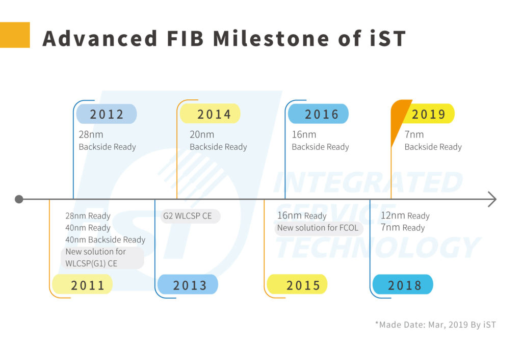
Image: The advanced FIB circuit editing milestone of iST.
Founded in 1994, iST began its business from IC circuit debugging and modification and gradually expanded its scope of operations, including Failure Analysis, Reliability Verification, Material Analysis, Automotive Electronic Verification Platforms and Signal Integrity Testing Services. iST has offered full-scope verification and analysis services to the IC engineering industry, its customers cover the whole spectrum of the electronics industry from IC design to end products.
In response to iST’s mission of providing integrated solutions to customers, iST not only focuses on its core laboratory services but also enters the mass production services of wafer backend process. http://www.istgroup.com