Issued Date: 2014/7/10
Issued By: iST
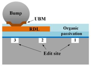
With specific preprocessing engineering methods, FIB circuit edit any sites covered by the bump (site 3), RDL (site 2), or organic passivation (site 1) can be achieved without problems.
Walking always ahead of times and industries, lab service provider Integrated Service Technology (iST) never stops in technology R&D. iST announced today new breakthrough in IC FIB circuit edit. With exclusive preprocessing engineering methods, iST has developed the second generation circuit edit solution for wafer-level chip scale package (WLCSP) to effectively shorten work time and enhance circuit edit success.
Four years ago, iST began developing the first generation WLCSP FIB circuit edit technology. First, it’s been published in the International Symposium Testing and Failure Analysis (ISTFA) organized by the ASM International. Later on, the Journal of Materials Science (J. Mater. Sci.) accepted and published it.
From the R&D phase, iST’s first generation WLCSP FIB circuit edit technology gradually entered the operation phase to successfully help many power management, analog, and multimedia IC design houses and mobile phone chipset developers to shorten the lead-time of product verification and debug and thereby ensure product launch just in time.
Continuing the success of the first generation, iST introduced this year the specific WLCSP circuit edit preprocessing engineering method. More importantly, we are honored to be invited by the International Symposium on the Physical and Failure Analysis of Integrated Circuits (IPFA), an IEEE-level event for semiconductor failure analysis, to present this second-generation WLCSP FIB circuit edit solution.
According to Dr. Sheng-yu Chen, manager of the Department of Material Analysis and FIB Engineering of iST, the aim of WLCSP is to finish IC packaging directly on the wafer using bump as a contact before the wafer is cut. Compared to traditional wire bonding packaging, WLCSP can effectively reduce packaging size. With the rise of wearable and smart handheld devices, WLCSP featuring smaller and thinner packaging size meets the trend of being slim and lightweight, thus fulfilling the demand of increasing clients.
“However, IC products packaged with WLCSP are confronted with two big challenges in FIB circuit edit. Most parts of circuits at the lower layers of an IC are covered by the bump and the RDL (redistribution layer) and cannot be edited. Even if there are circuits not covered by the bumps and RDLs, as the organic passivation on top is thicker, greater effort and more time is needed to edit these circuits,” added Dr. Chen.
The second-generation WLCSP circuit edit technology is the solution for these products. With specific preprocessing engineering methods, circuits under the bump, RDL, or organic passivation can be edited without problems (see Figure 1). Compared to the first generation circuit edit method using metal conductors, the second-generation WLCSP circuit edit technology can significantly reduce editing time by 50% and double the yield rate.
In addition to the research achievements in advanced IC packaging, iST never stops developing process technology. For example, it has recently purchased the FEI V400ACE FIB equipment with excellent resolution and stability to edit the circuits of ICs packaged with 16µm process.
By upgrading R&D technology and equipment, iST hopes to help IC designers requiring advanced packaging to act more straightforwardly, swiftly, and fast in circuit verification, debug, and failure analysis, so as to shorten the time to market.
If you need our verification service, please feel free to contact Brian Wang at 886-3-579-9909 ext. 8886 or mail toSales@istgroup.com
About Integrated Service Technology
Founded in 1994, iST began its business from IC circuit debugging and modification and gradually expanded its scope of operations to include failure analysis, reliability verification, material analysis, and quality assurance. Through the years, iST has constructed a comprehensive verification and analysis engineering platform, offering full-scope services to the IC engineering industry. iST customers cover the whole spectrum of the electronics industry from IC design to end products.
In response to rising environmental awareness, iST not only focuses on its core services but is also expanding its service offerings based on international trends. iST’s lead-free and halogen-free verification testing, chemical quantitative testing and signal integrity services have all been accredited by multiple international independent third-party organizations including TUV NORD Germany and BSI UK. With increased outsourcing by major international brands, iST now also plays the role of independent quality testing laboratory for OBM outsourcing products and is certified by Dell, Cisco, Delphi, Continental Automotive and Lenovo.
Headquartered in Hsinchu, iST’s pursuit of precision, perfection and efficiency has led it to expand its operations around the world. The iST Group now includes iST Kunshan, iST Shanghai, iST Beijing and iST Shenzhen in China, IC Service in Japan, and an iST laboratory in the US. These are all dedicated to providing customers with prompt, reliable and high-quality technical services in order to grow with the leaders of the world. For more information, please visit the iST website at:www.istgroup.com