5G is Coming Soon: Are You Ready for Relevant Packaging Test Items?

Looming 5G is Leading the Development of Semiconductor Industry
Thanks to soaring growth pushed by 5G commercialization around the world, 5G relevant devices are expected to flood global markets, including network infrastructure, networking equipment and nodes, and mobile terminals.
5G products are much more demanding in their design due to advanced technical specification covering faster network speed, higher frequency band, scaled up connection, shorter network latency, and more robust network reliability. To meet performance and technical specification, they demand improved designs of chips, structure, and system along with good product verification, test, and analysis.
Advanced Packaging Technology Resolves 5G Chip Performance Requirements
The 5G technology is aimed at higher speed, higher transmission capacity and lower latency. How to hit these goals? The higher the 5G chip performance is, the larger the technology’s demand is. It could be developed in two aspects:
- Technology Scaling : Reduce the L/S (Line/Space) to fasten computing speed in the limited space.
- Advanced Packaging : To tackle with issues of product dimension, power consumption, and heat dissipation as well as to embed antennas in package for improved speed.
Since “technology scaling” brings along increasing equipment installation costs and challenging yield and technology demands. The second option, “advanced packaging” is now the focus to better performance, reduce process costs, and break physical limits.

This may be reviewed in terms of terminal and cloud applications addressing the advanced packaging needs of 5G devices:
Advanced Packaging Needs of Terminal Devices
Terminal devices include smartphone and notebook. The 5G smartphone, for instance, is focused on the smaller dimension and the faster transmission. And the overall performance depends on AP(Application Processor). Along with 5G high frequence coming, the design of antenna certainly needs to be adjusted.
Let’s take the 5G smartphone application processor and antenna as examples for illustration.
1. Application Processor (AP) for 5G Smartphones
In addition to scaling of wafer technology, the AP performance is also relied on the assistance of package technology.With regard to packaging form, the mainstream is POP (Package on Package), which can effectively reduce package dimension and increase the transmission speed.
The connection methods are evolved from the conventional wire bonding and flip chip to fan-out technology. The latter lessens the use of a substrate with RDL wiring as shown in the figure below.
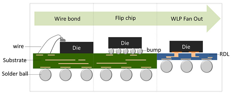
The fan-out technology can lessen the use of a substrate which, in turn, improves performance and heat dissipation while reducing product’s dimension and costs. This makes fan-out POP packaging the first choice for ICs of AP.
2. Antenna
Devices are placing more demands in terms of antenna dimension, path loss, and signal’s accuracy on 5G devices as the latter are commercializing the high-frequency mmWave (millimeter wave) and stretching the frequency of 5G signals from under 1GHz to over 30GHz.
- Dimension of Antenna: Antenna volume is determined by frequency. With the use of a higher frequency like mmWave, the antenna dimension may get contracted to the range of millimeter scale.
- Signal’s Accurancy: The more antennas for signal ins and outs may speed up data transmission and make sure data accurancy.
- Path Loss: High-frequency waves come with better penetration at the cost of shorter transmission distance due to energy losses and interference.
To cram more antennas in the limited space available, the Antenna in Package (AiP) packaging form becomes the ideal solution which contains RF chips in a System in Package (SiP) or PoP structure to reduce chip dimension and transmission distance for less energy losses. The location of RF chips can be used to differentiate the structure into two types: One is a structure that has RF chip contained in the substrate, and the other is a structure has RF chip placed outside the substrate.
Advanced Packaging Needs of Cloud Devices
Cloud devices include base stations and servers, are aimed at dealing with huge amounts of data and messages. Focusing on high performance and heat dissipation, they are built upon HPC chips and employ 2.5D/3D packaging for improved signal transmission speed and quality.
The inter-die communication bridged by the combination of silicon interposer, RDL and PCB substrate, they benefit by a 4–5 times smaller L/S(Line/Space) when compared to conventional substrate as shown in the figure below.
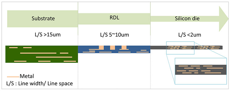
A smaller L/S(Line/Space) can add more pin counts in package and reduce signal latency for better total system performance.

DO NOT Overlook the Challenges in Technology and Verification Analysis Imposed by Looming 5G Chip Heterogeneous Integration
Changes in packaging structure and material will bring impacts on reliability and production outcome, including CTE mismatch, warpage, and SMT. All these may result in issues in board level reliability test.
Technology Challenge
1. CTE Mismatch
Different materials have different coefficients of thermal expansion (CTE). Changes in temperature could result in varying expansion. Owing to the heterogeneous integration of 5G advanced packaging, the stress release probably leads to cracking or delamination and affects the operation of the chip.
“Heat” is always the key factor in determining product reliability. This is especially the case when chips of varying temperature resistance are contained in one package. The same may hold for a chip’s external and system temperature.
2. Warpage
The 5G advanced packaging tends to get severe warpage due to more complex heterogeneous integration based chip staking and increasingly larger package dimension. This is especially the case with SMT as its high temperature may lead to more severe warpage and harder soldering to the PCB.
3. Others
The 2.5D IC and 3D IC packaging usually apply on product required high performance and high efficiency, may come with a heat sink to address heat dissipation and warpage. Nevertheless, the heavier weight of heat sink is easily to flatten the solder ball during the SMT process, which may lead to bridge and other problems.
The Verification Analysis Over Chips By 5G Advanced Packaging
The R&D of 5G chips by advanced packaging requires detailed verification covering their warpage level, analysis over materials for heterogeneous integration, status of solder balls in SMT process, and impact on solder balls and silicon interface layers under the change of temperature.
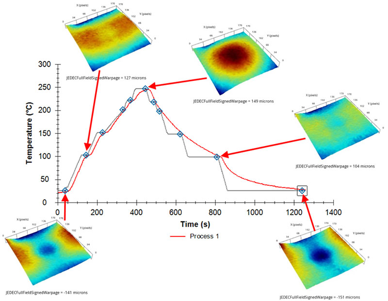
1. Severe Warpage Causes SMT Failure and Test Issues
Increasing design complex in products by advanced packaging and larger dimension may result in more severe product warpage which, in turn, may tamper with the SMT results and create issues in testing socket contact.
iST is providing a shadow moire to address this issue by simulating the warpage level of components and PCBS during the reflow process. The results are then used to set up SMT operation and ensure good soldering quality of SMT.
2. CTE Mismatch Verification
After long term operation the interface of component materials may exhibit internal stress due to CTE mismatch caused by changes in temperature, which will result in delamination and cracking and hamper component operation. The environmental reliability test, including uHAST, TCT, Multi-reflow and other simulation for actual operation can be used to ensure the components’ good operation in spite of changes in material and design in the future.
iST is providing services for reliability test specification consulting and subsequent failure analysis services to help customers to identify causes of component errors.
3. Complex Structure Of Advanced Packaging is Hampering its Conventional Tests
Changes in package structure is preventing the conventional tests (e.g. 2D x-ray, SAT, and FIB) from detecting delamination and other electric test defiant errors. Addressing this, iST is providing complete recommendations to specific packaging structure, e.g. the 2.5D IC packaging, to ensure thermal grease from delamination after reflow.