Issued Date: 2019/8/6 Warpage
Issued By: iST
Reliability test failure after ICs mounting on PCB
Due to solder empty and early failure caused by warpage
Can this be prevented by embracing simulated warpage status before SMT?
The nightmare in IC design is reliability test failure after ICs SMT while the quality of ICs is in good condition. The iST board level reliability (BLR) lab has witnessed this quite often with its clients. Post-SMT warpage is most commonly found lately. This not only leads to early reliability failure, but also may result in having to return the product back to its initial and time-consuming IC design stage. Compared to repeated debugging and redesign of ICs, it’s worse when the deadline of delivery to downstream system customers is approaching and there is no way out.
What Leads to Warpage?
Why is warpage-oriented reliability failure occurring more frequently recently? The iST BLR lab found this is a result of more and more manufacturers’ efforts in developing ICs by advanced process. The latter requires stacking ICs, e.g. MCM (multi-chip module), SiP (system in package), and Fan-in/Fan-out of different materials and functions. They employ components of quite comprehensive and diversified materials which results in warpages due to the different coefficient of thermal expansion (CTE) of substances when stacked together (Figure 1).
Warpages suffered by IC components may ramp up when being mounted on PCBs due to different CTEs between ICs and PCBs. Once the situation tips over certain limit the SMT soldering quality may become hampered which, in turn, leads to poor reliability in future.
It’s quite a technical challenge to stack substances of different temperature characteristics in good order and prevent inter-affection during heating and radiating.
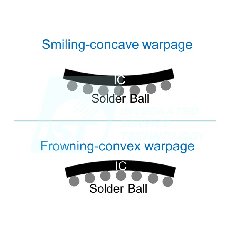
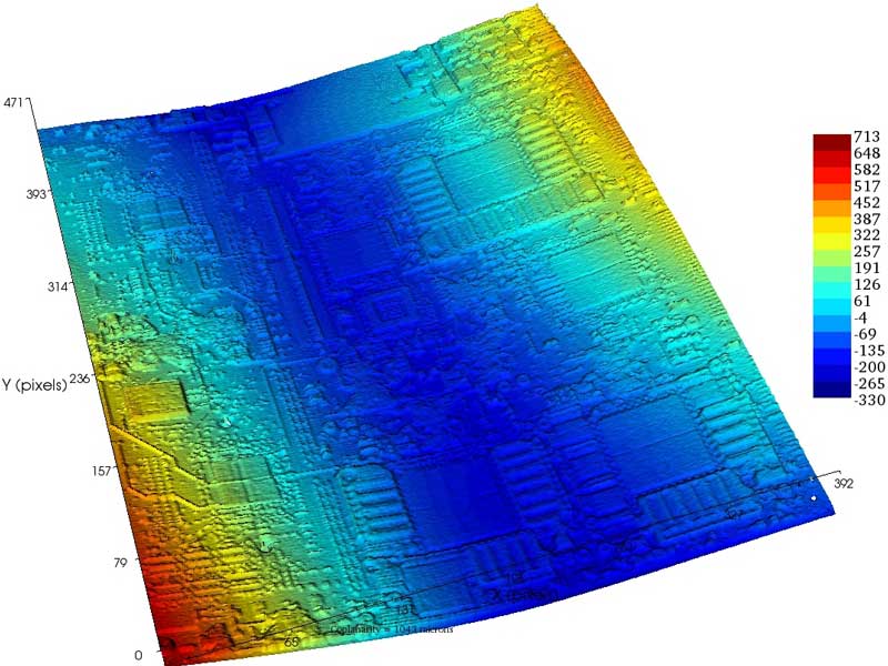
Figure 1: ICs subject to advanced processes would end up with warpages more or less. This should have no impact on post-SMT component quality as long as the warpage level is controlled within the IPC specification (photo courtesy of Akrometrix).
Complex stacking of IC components materials in advanced processes may lead to out of control warpage
5-10 years ago, the warpage amount was controlled in a range of 6-8mil and was less likely to hamper the SMT process later. Thanks to complex material types and repeated stacking required by advanced processes, the temperature induced warpage amount is getting more serious than samples 5-10 years earlier. The iST BLR lab projects that stencil, design to bond solder paste and solder ball successfully, is getting thinner with increasing pin counts when SMT ICs to PCBs (Figure 2, 3, and 4). It’s quite unlikely that the warpage amount in a range of 6-8mil could maintain the SMT process quality as in the early days.
Figure 2: SMT process with solder paste stuffed through stencil to integrate IC with solder ball
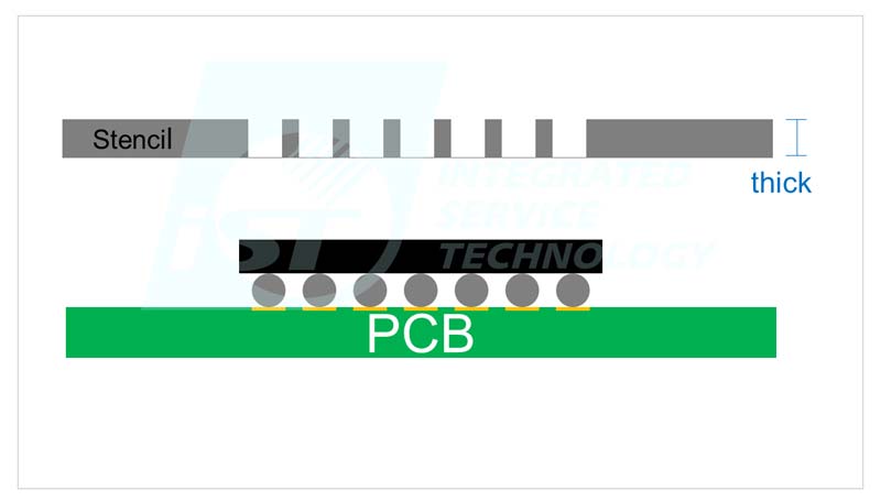
Figure 3: Conventional PCB and stencil can be relatively thick due to fewer pin counts and solder balls
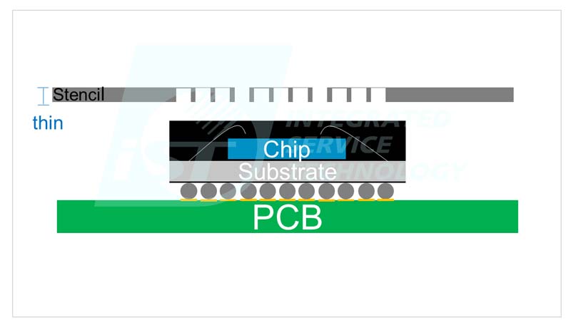
Figure 4: The advanced process mandates thinner stencils due to a greater pin counts and solder balls
Solder empty and short circuit due to over warpage after ICs SMT to PCB
PCBs warp the same as their components do. Contradicting conventional wisdom, PCBs thicker than 1.6mm are likely to warp. A typical case encountered by iST’s BLR lab falsely assumed that only ICs warped when SMTed on the PCB (Figure 5 and 6). iST made a series of SMT process parameter changes and failed to tackle the problem. Eventually, it concluded that not only ICs, but also the PCB warped, at quite large levels as shown in figure 7, and resulted in the SMT anomaly.
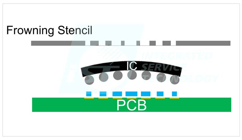
Figure 5: Frowning warpage components go with frowning stencil
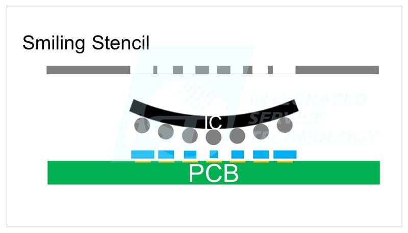
Figure 6: Smiling warpage components go with smiling stencil
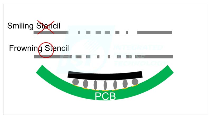
Figure 7: Contradicting the assumption that the PCB warps little, the actual measurements suggest that its warpage outruns those of its components. In cases like this, smiling warpage components have to go with frowning rather than smiling stencil. That is, the warpages of a PCB may lead to the SMT abnormality.
Reliability verification remains failed after solder empty and short circuit solved
Worse than the solder empty and short circuit is that solder joints after warpage may get stretched or squeezed into “thin and tall” (figure 9) or “short and fat” (figure 10) rather than the “ball” like (figure 8) forms. These “non-ball” spots may get broken by concentrated stress which pushes up the rate of early failure in later reliability verification.
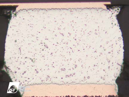
Figure 8: Perfect ball-like solder joint
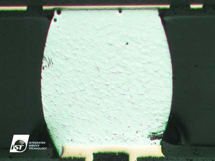
Figure 9: Thin and tall solder joint
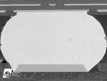
Figure 10: Short and fat solder joint
Changing sizes of openings on the SMT stencil mitigates stretching and stressing of solder joints
There are two approaches in dealing with warpage in the SMT process: one is to change the size of openings on stencil to give more solder paste at sections of greater spacing; the other is to control component deformation by the jig. Both require repeated trial and error to optimize the SMT. In worst cases; it may have to go back to the design stage to use alternative substances and waste a lot of time.
Simulate and measure warpage amount to prevent SMT anomaly and have reliability tested successfully
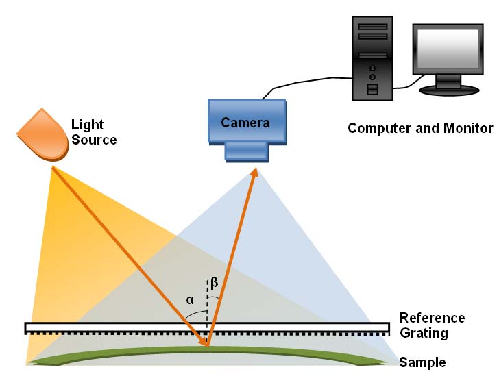
It’s better to get the IC and PCB warpage relevant data before SMT. With warpage measurement relevant equipment, the iST BLR lab can simulate warpage suffered by the IC and PCB (figure 11) to change SMT parameter settings and ensure soldering quality in the SMT process to prevent reliability test failure and wasted costs.
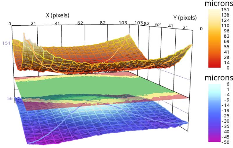
Figure 11: Simulate and analyze components and PCBs before SMTing to learn about warpages in advance (courtesy of Akrometrix).
It took just about 30 minutes to complete the measurement and analysis operation and get the warpage amount of components in different temperatures. It may simulate the environment of temperature cycle to help customers find the suitable reliability test plan, and get the temperature which results in the maximum warpage of the product, and manage to improve and prevent warpage during tests.
Warpage is measured by generating the Moire pattern distribution diagram based on the geometric interference between the reference gratings and their shadows on the samples and calculating the relative vertical displacement in each pixel position. This may be used to simulate SMT reflow temperature and operating environment conditions while logging the entire warpage displacement cycle.
(Photo courtesy: Akrometrix)
Post-SMT warpages have been being detected by iST’s BLR lab. We have no means to tackle with it as this it is caused by characteristics came with the material used. However, we may find the perfect warpages ratio by screening out components and PCBs of the same warpages direction to maintain reliability level and create a total value greater than the sums of its parts.
Should you have any inquires for SMT or warpages, please call Daniel Chuang at +886-3-579-9909 Ext. 6406 or send an email to web_BLR@istgroup.com.