Issued Date: 2021/07/06
Issued By: iST
Facing the IC industry’s advanced process development; iST today (July 6, 2021) announced another breakthrough in IC circuit edit technology! Its backside FIB circuit editing technology can now apply to 5 nm processes. After successfully edited samples of 7 nm process for the first time in 2018, iST is now challenged to edit circuits of still more advanced processes to help clients in optimizing chip performances and shorten the product launch cycle.
iST explains why IC designers need to carry out circuit edit. With rising costs in developing advanced processes and longer lead time caused by shortage in wafer production capacity, chips are more likely to miss the design target even when EDA and other circuit simulation software are getting better day by day. New masks for revised circuit not only cost more but also wastes more than one month for new chips to come out. Most IC design houses then choose to edit the IC circuits to ensure the latter’s compliance with the design specifications by spending fewer bucks and waiting for hours not tens of days.
The FIB electron microscope accelerates GA+ primary beam with an electric field into ion beams before hitting the sample surface to sputter secondary ions or electrons for imaging. By airing different gases when hitting the surface, the circuits would be edited as materials on chip surface are selectively etched at faster or slower speed and conductive and dielectric insulating materials are deposited to them. With the aid of the CAD navigation system and accurate positioning, the circuits are edited more precisely. iST further pointed.
Being the first private lab in Taiwan offering FIB circuit editing service, iST is revolutionizing the verification model accepted by IC design houses by cutting huge amount of times and costs spent in moving a product from concept design to mass production. The iST exclusive FIB circuit editing skills, it is now mature in editing 5nm circuit from the backside. The latest equipment launched in Q1 betters the insulation effects with higher resistivity (1E15 uΩ-cm) of dielectric material and challenges the more advanced process by raising image resolution from 4.5nm to 3.5nm and improving the success rate in editing circuits of very thin wires and greater complexity at a deeper location
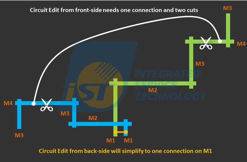
Figure : Diagram for path tracking, let’s assume that this advanced process is 9M+AP. It’s very difficult to edit the M4 from chip’s front side as this requires going through 6 metal layers (AP~M5). Instead, editing from the back side not only reduces the number of layers to go through (just one Active Area layer) but also can simplify the editing on M1.
PSI’s Patent
About Integrated Service Technology
Founded in 1994, iST began its business from IC circuit debugging and modification and gradually expanded its scope of operations, including Failure Analysis, Reliability Verification, Material Analysis, Automotive Electronic Verification Platforms and Signal Integrity Testing Services. iST has offered full-scope verification and analysis services to the IC engineering industry, its customers cover the whole spectrum of the electronics industry from IC design to end products.
In response to rising Cloud Intelligence, Internet of Things (IoT) and Internet of Vehicles (IoV), iST not only focuses on its core services but is also expanding its service offerings based on international trends, such as automotive electronic verification platforms, signal integrity testing services.http://www.istgroup.com